|
|
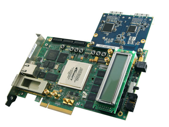
The Stratix V GX FPGA Video Development System fills the need for the highest bandwidth, best performance video applications. The kit features an extensive feature-set of memories, including DDR3, QDRII+, and RLDRAM II. The QSFP optical cage, PCIe x8 edge connectors, SDI, and gigabit Ethernet options allow for blazingly fast interfacing with peripherals.
The DVI-HSMC daughter card part of the bundled package will allow developers to access high quality and high resolution video signals that can support resolution up to 1600x1200. A complete DVI video controller design with source code is provided.
Terasic recognized for its strong design expertise in high-end video, imaging and multimedia products have made available a video development package that targets video processing development. The platform can also allow users to experience advanced image processing designs incorporating VIP (Altera’s Video and Image Processing Suite MegaCore Functions).
Stratix V GX Video Development System
Featured device:
- Stratix V GX FPGA: 5SGXEA7K2F40C2N
Configuration, status, and setup elements
- JTAG
- On-board USB-BlasterTM II cable
- Fast passive parallel (FPP) configuration via MAX® V device and flash memory
- One reset config push button
- One CPU reset push button
- Two configuration push buttons
Clocks
- 50-MHz, 125-MHz, 100-MHz, and 148.5-MHz programmable oscillators
- SMA input (LVPECL)
General user input and output
- 10/100/1000Mbps Ethernet PHY (SGMII) with RJ-45 (copper) connector
- 16x2 character LCD
- One 8-position dual in-line package (DIP) switch
- Sixteen user LEDs
- Three user push buttons
Memory devices
- DDR3 SDRAM (1,152 MB, x72-bit wide)
- QDR II+ SRAM (4.5 MB, 2-Mb x18-bit wide)
- Footprint compatible to QDR II 4-Mb x18-bit wide
- RLDRAM II (72-Mbyte CIO RLDRAM II with an 18-bit data bus)
Component and interfaces
- PCIe x8 edge connector
- Two HSMC connectors
- SMB for serial digital interface (SDI) input and output
- QSFP optical cage
- 10/100/1000Mbps Ethernet PHY (SGMII) with RJ-45 (copper) connector
Power
- Laptop DC input
- PCIe edge connector
- Nios® II processor web server and remote system update
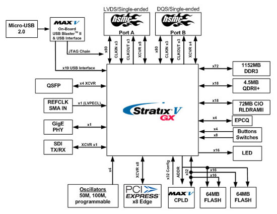
Stratix V GX FPGA Development Board Block Diagram
Terasic DVI-HSMC Card
Digital Transmitter
- One DVI transmitter with single transmitting port
- Digital Visual Interface (DVI) Compliant
- Supports resolutions from VGA to UXGA (25 MHz – 165 MHz Pixel Rates)
- Universal Graphics Controller Interface
- 12-Bit, Dual-Edge and 24-Bit, Single-Edge Input Modes
- Adjustable 1.1 V to 1.8 V and Standard 3.3 V CMOS Input Signal Levels
- Fully Differential and Single-Ended Input Clocking Modes
- Standard Intel 12-Bit Digital Video Port Compatible as on Intel™ 81x Chipsets
- Enhanced PLL Noise Immunity
- On-Chip Regulators and Bypass Capacitors for Reducing System Costs
- Enhanced Jitter Performance
- No HSYNC Jitter Anomaly
- Negligible Data-Dependent Jitter
- Programmable Using I²C Serial Interface
- Single 3.3-V Supply Operation
Digital Receiver
- One DVI receiver with single receiving port
- Supports UXGA Resolution (Output Pixel Rates Up to 165 MHz)
- Digital Visual Interface (DVI) Specification Compliant
- True-Color, 24 Bit/Pixel, 16.7M Colors at 1 or 2-Pixels Per Clock
- Laser Trimmed Internal termination Resistors for Optimum Fixed Impedance Matching
- 4x Over-Sampling
- Reduced Ground Bounce Using Time Staggered Pixel Outputs
- Lowest Noise and Best Power Dissipation Using TI PowerPAD™ Packaging
|
|
|


