|
|
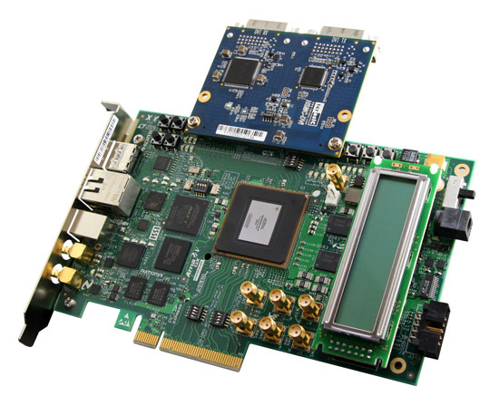
The Arria V GX FPGA Video Development System is an ideal video processing platform for high-performance, cost-effective video applications. The Arria II development kit features 256MB of SDRAM memory, HDMI, and SDI connections to form a perfect solution for imaging applications.
The DVI-HSMC daughter card part of the bundled package will allow developers to access high quality and high resolution video signals that can support resolution up to 1600x1200. A complete DVI video controller design with source code is provided.
Terasic recognized for its strong design expertise in high-end video, imaging and multimedia products have made available a video development package that targets video processing development. The platform can also allow users to experience advanced image processing designs incorporating VIP (Altera’s Video and Image Processing Suite MegaCore Functions).
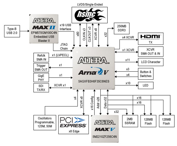
Altera Arria V GX Video Development System
FPGA:
- Arria V GX 5AGXFB3H4F35C5NES
System controller: MAX® V 5M2210ZF256C4N
- Power monitor GUI
- Single analog-to-digital converter (ADC), eight channels
- Non-isolated power rail
- Fast passive parallel (FPP) x16 mode through parallel flash loader (PFL)
- Control and status registers
Embedded USB-BlasterTM II:
HDMI 1.3 TX
- x4 XCVR, 2.7 Gbps (max by level shifter) and 270 MHz TX clock HDMI TX connector
- STMicroelectronics HDMI level shifter STHDLS101T
- Level shift XCVR PCML 1.5V <-> TMDS level
- DDC and HPD <-> HDMI compliant level
- Data channel up to 2.7 Gbps; HDMI 1.3 compliant
- Clock channel up to 270 MHz; enough to support 2.7 Gbps data rate
- HDMI specification: clock period = 10x of UI
SDI 3G
- x1 XCVR TX/RX loopback
- x2 SMB connectors and cable (cable not included in kit)
- Up to 2.97 Gbps
- Uses National Semiconductor driver/receiver LMH0384SQ/LMH0303SQx
- Requires 148.5 MHz and 148.35 MHz at XCVR refclk to support US and EU standard respectively
- Use VCXO to fine tune and lock to the recovered CDR frequency
HSMC
- x8 XCVR up to 6.375 Gbps
- Not complied to PCI Express® (PCIe® ) HIP pin assignment
- x4 CMOS
- x8 TX and x9 RX differential interface using dedicated TX/RX channels
- x2 low-voltage differential signalling (LVDS) clock in
- x2 differential clock out
- I2C
- JTAG
- Minimum current support
- 2A @ 3.3V
- 1A @ 12V
- Dedicated clock domain from Si 5338 clock generator for xcvr refclk
- HSMC loopback with BTS GUI
SMA
- 1x XCVR TX/RX channel
- 1x LVPECL clock input
- 1X LVPECL clock output
Clocking
- Dedicated clock domain from Si 5338 clock generator for xcvr refclk
DDR3 SDRAM x32
- Micron MT41J64M16LA-15E DDR3 SDRAM 8MX16X8
- Two devices: 2 x16 width = x32
- BTS DDR3 SDRAM GUI using Uniphy and high performance (HP) controller II
SSRAM
- 512k x36, 18 Mb ISSI IS61VPS51236A
- Shared address or data with flash
User IO
- LCD character
- x4 DIP switch
- x3 PB
- x4 LED
Configuration
- FPP x16 mode
- Dual flash 512Mbit Numonyx PC28F512P30BF (52 MHz FMAX )
- JTAG header
Embedded USB Blaster II
- Cypress Microcontroller CY7C68013A as USB PHY 2.0
- MAX II
Ethernet
- 10/100/1000 Base-T
- RJ-45 connector, on-board LED for link status
- Marvell Ethernet PHY 88E1111
- Requires 50 MHz clock from CLKIN
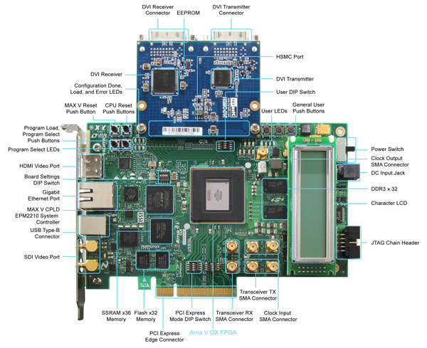
Altera Arria V GX Starter Board Block Diagram
Terasic DVI-HSMC Card
Digital Transmitter
- One DVI transmitter with single transmitting port
- Digital Visual Interface (DVI) Compliant
- Supports resolutions from VGA to UXGA (25 MHz – 165 MHz Pixel Rates)
- Universal Graphics Controller Interface
- 12-Bit, Dual-Edge and 24-Bit, Single-Edge Input Modes
- Adjustable 1.1 V to 1.8 V and Standard 3.3 V CMOS Input Signal Levels
- Fully Differential and Single-Ended Input Clocking Modes
- Standard Intel 12-Bit Digital Video Port Compatible as on Intel™ 81x Chipsets
- Enhanced PLL Noise Immunity
- On-Chip Regulators and Bypass Capacitors for Reducing System Costs
- Enhanced Jitter Performance
- No HSYNC Jitter Anomaly
- Negligible Data-Dependent Jitter
- Programmable Using I²C Serial Interface
- Single 3.3-V Supply Operation
Digital Receiver
- One DVI receiver with single receiving port
- Supports UXGA Resolution (Output Pixel Rates Up to 165 MHz)
- Digital Visual Interface (DVI) Specification Compliant
- True-Color, 24 Bit/Pixel, 16.7M Colors at 1 or 2-Pixels Per Clock
- Laser Trimmed Internal termination Resistors for Optimum Fixed Impedance Matching
- 4x Over-Sampling
- Reduced Ground Bounce Using Time Staggered Pixel Outputs
- Lowest Noise and Best Power Dissipation Using TI PowerPAD™ Packaging
Documents
| Arria V GX Starter Board Reference Manual (PDF) |
- |
|
2013-01-07 |
 |
| Arria V GX Starter Kit User Guide (PDF) |
- |
|
2013-01-07 |
|
CD-ROM
| DVI Combo CD-ROM |
- |
|
2013-02-01 |
 |
| Kit installation |
- |
|
2013-01-07 |
|
Please note that all the source codes are provided "as is". For further support or modification, please contactTerasic Support and your request will be transferred to Terasic Design Service.More resources about IP and Dev. Kit are available on Altera User Forums. |
|
|


