|
|
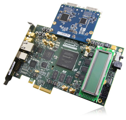
The Cyclone V GX Video Development System is an ideal video processing platform for high-performance, cost-effective video applications. With PCIe x4 lanes and high-speed 3.125 Gbps transceiver capabilities, the Cyclone V GX kit allows for a myriad of functionalities such as prototyping, power measurement, and high-speed communication. Memory interfaces include flash memory, SRAM, and DDR3, creating a complete integrated memory interface solution for memory-intensive applications.
The DVI-HSMC daughter card part of the bundled package will allow developers to access high quality and high resolution video signals that can support resolution up to 1600x1200. A complete DVI video controller design with source code is provided.
Terasic recognized for its strong design expertise in high-end video, imaging and multimedia products have made available a video development package that targets video processing development. The platform can also allow users to experience advanced image processing designs incorporating VIP (Altera’s Video and Image Processing Suite MegaCore Functions).
Altera Cyclone V GX FPGA Development Board
Featured devices
- Cyclone V GX FPGA - 5CGXFC7D6F31C7NES
- MAX ® V CPLD - 5M2210ZF256C4N (system controller)
- MAX II CPLD - EPM240M100C4N (embedded USB-BlasterTM II)
- MAX II CPLD- EPM240M100C4N (optional, third party security CPLD feature)
Configuration
- Embedded USB-Blaster II (JTAG)
- Fast Passive Parallel (PFL)
- Push buttons, DIP switches and LEDs
Memory devices
- Two banks x40 bit DDR3 SDRAM with error correction code (ECC)
- 512Mb flash memory and 18MB SRAM
Standard communication ports
- USB 2.0
- Gigabit Ethernet
- PCIe x4 Edge Connector
- Universal high-speed mezzanine card (HSMC) (x 4 Xvcrs, x16 Tx LDVS, x16 Rx LVDS)
- One serial digital interface (SDI) channel
- Two SMAs for one transceiver channel
Clocking
- Programmable clock generator for FPGA reference clock input
- 125 MHz LVDS oscillator for FPGA reference clock input
- 148.5/148.35 MHz LVDS VCXO for FPGA reference clock input
- 50 MHz single-ended oscillator for FPGA and MAX V FPGA clock input
- 100-MHz single-ended oscillator for MAX V FPGA configuration clock input
- SMA input (LVPECL)
Power
- Laptop DC Input 14 – 20V adapter
- PCIe Edge Connector
System Monitoring Circuit
- Power (Voltage, Current, Wattage)
Mechanical
- PCIe card standard size (6.600" x 4.199")
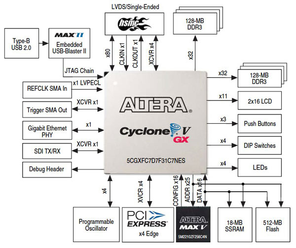
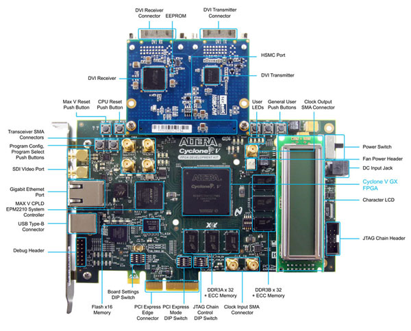
Altera Cyclone V GX FPGA Development Board Block Diagram
Terasic DVI-HSMC Card
Digital Transmitter
- One DVI transmitter with single transmitting port
- Digital Visual Interface (DVI) Compliant
- Supports resolutions from VGA to UXGA (25 MHz – 165 MHz Pixel Rates)
- Universal Graphics Controller Interface
- 12-Bit, Dual-Edge and 24-Bit, Single-Edge Input Modes
- Adjustable 1.1 V to 1.8 V and Standard 3.3 V CMOS Input Signal Levels
- Fully Differential and Single-Ended Input Clocking Modes
- Standard Intel 12-Bit Digital Video Port Compatible as on Intel™ 81x Chipsets
- Enhanced PLL Noise Immunity
- On-Chip Regulators and Bypass Capacitors for Reducing System Costs
- Enhanced Jitter Performance
- No HSYNC Jitter Anomaly
- Negligible Data-Dependent Jitter
- Programmable Using I²C Serial Interface
- Single 3.3-V Supply Operation
Digital Receiver
- One DVI receiver with single receiving port
- Supports UXGA Resolution (Output Pixel Rates Up to 165 MHz)
- Digital Visual Interface (DVI) Specification Compliant
- True-Color, 24 Bit/Pixel, 16.7M Colors at 1 or 2-Pixels Per Clock
- Laser Trimmed Internal termination Resistors for Optimum Fixed Impedance Matching
- 4x Over-Sampling
- Reduced Ground Bounce Using Time Staggered Pixel Outputs
- Lowest Noise and Best Power Dissipation Using TI PowerPAD™ Packaging
Documents
| Cyclone V GX FPGA Development Kit User Guide (PDF) |
- |
|
2013-01-08 |
 |
| Cyclone V GX FPGA Development Board Reference Manual (PDF) |
- |
|
2013-01-08 |
|
CD-ROM
| DVI Combo CD-ROM |
- |
|
2013-02-01 |
 |
| Kit installation |
- |
|
2013-01-08 |
|
- Cyclone V GX FPGA Development Kit software content
- Design examples
- PCIe loop back and reference design
- Board test system (BTS)*
- Board update portal (BUP)*
- Includes Nios® II embedded soft processor and Ethernet
- Complete documentation (see Resources)
- Free software supported by Quartus® II software v12.0 SP2, Web Edition
|
|
|


