|
|
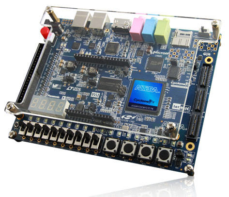
The Cyclone V Starter Kit presents a robust hardware design platform built around the Altera Cyclone V GX FPGA, which is optimized for the lowest cost and power requirement for transceiver applications with industry-leading programmable logic for ultimate design flexibility. With Cyclone V FPGAs, you can get the power, cost, and performance levels you need for high-volume applications including protocol bridging, motor control drives, broadcast video converter and capture cards, and handheld devices. The Cyclone V Starter Kit development board includes hardware such as Arduino Header, on-board USB Blaster, audio and video capabilities and much more. In addition, an on-board HSMC connector with high-speed transceivers allows for an even greater array of hardware setups. By leveraging all of these capabilities, the Cyclone V Starter Kit is the perfect solution for showcasing, evaluating, and prototyping the true potential of the Altera Cyclone V GX FPGA.
|
* Power Solution

|
* Memory Solution

|
* Clock Solution

|
|
| |
|
|
* Capacitive Component Solution

|
* Analog-to-Digital Converter Solution

|
* Low Power Memory Solution

|
|
| |
|
|
* Inductive Component Solution

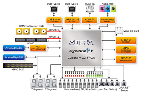
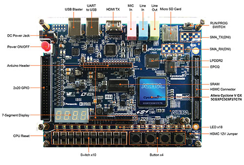
FPGA Device
- Cyclone V GX 5CGXFC5C6F27C7N Device
- 77K Programmable Logic Elements
- 4884 Kbits embedded memory
- Six Fractional PLLs
- Two Hard Memory Controllers
- Six 3.125G Transceivers
Configuration and Debug
- Quad Serial Configuration device – EPCQ256 on FPGA
- On-Board USB Blaster (Normal Type-B USB connector)
- JTAG and AS mode configuration supported
Memory Device
- 4Gb LPDDR2 x32 bits data bus
- 4Mb SRAM x16 bits data bus
Communication
Expansion I/O
- HSMC x 1, including 4-lanes 3.125G transceiver
- 2x20 GPIO Header
- Arduino header, including analog pins
- SMA x 4 (DNI), one-lane 3.125G transceiver
Display
- HDMI TX, compatible with DVI v1.0 and HDCP v1.4
Audio
- 24-bit CODEC, Line-in, line-out, and microphone-in jacks
Switches, Buttons, LED, and 7-Segments
- 18 LEDs
- 10 Slide Switches
- 4 Debounced Push Buttons
- 1 CPU reset Push Buttons
- Four 7-Segments
Micro SD Card Socket
- Provides SPI and 4-bit SD mode for SD Card access
Power
Block Diagram
Documents
| User Manual |
V.1.0.0 |
8276 |
2013-07-24 |
 |
CD-ROM
| System CD-ROM |
V.1.0.0 |
|
2013-07-24 |
 |
Please note that all the source codes are provided "as is". For further support or modification, please contactTerasic Support and your request will be transferred to Terasic Design Service.More resources about IP and Dev. Kit are available on Altera User Forums.
|
| |
|
|


