|
|

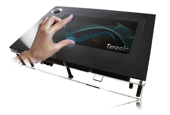
The Video and Embedded Evaluation Kit - Multi-touch on Cyclone® V SoC Development Board (VEEK-MT-C5SoC) is a comprehensive design environment with everything embedded developers need to create processing-based systems. VEEK-MT-C5SoC delivers an integrated platform that includes hardware, design tools, intellectual property (IP) and reference designs for developing embedded software and hardware platform in a wide range of applications. The fully integrated kit allows developers to rapidly customize their processor and IP to best suit their specific application. The VEEK-MT-C5SoC features the Altera Cyclone® V SoC development board targeting the Altera Cyclone® V SX SoC FPGA, as well as a capacitive LCD multimedia color touch panel which natively supports multi-touch gestures. A 5-megapixel digital image sensor, ambient light sensor, and 3-axis accelerometer make up the rich feature-set. The all-in-one embedded solution offered on the VEEK-MT-C5SoC, in combination of the LCD touch panel and digital image module, provides embedded developers the ideal platform for multimedia applications with unparallel processing performance. Developers can benefit from the use of FPGA-based embedded processing system such as mitigating design risk and obsolescence, design reuse, reducing bill of material (BOM) costs by integrating powerful graphics engines within the FPGA, and lower cost. - ARM Development Studio 5 (DS-5™) Altera Edition Toolkit
- Hardware-to-software handoff tools
- Linux run-time software for application development
- SoC hardware libraries for firmware development
- Application example
Cyclone V SX SoC—5CSXFC6D6F31C6N (SoC)- 110K LEs, 41509 ALMs
- 5140 M10K memory blocks
- 224 18x18 Multiplier
- 6 FPGA PLLs and 3 HPS PLLs
Configuration Device and USB Blaster Circuit- Active Serial (AS) x1 or x4 configuration (EPCQ256SI16N)
- MAX® V CPLD (5M2210ZF256I5N) in a 256-pin FBGA package as the System Controller
- Flash fast passive parallel (FPP) configuration
- MAX II CPLD (EPM570GM100) as part of the embedded USB-BlasterTM II for use with the Quartus® II Programmer
Memory Devices- One 1,024-Mbyte (MB) HPS DDR3 SDRAM with error correction code (ECC) support
- One 1,024-MB FPGA DDR3 SDRAM
- One 256-Megabit (Mb) quad serial peripheral interface (QSPI) flash
- One 512-Mb CFI flash
- One 32-Kb I2C serial electrically erasable PROM (EEPROM)
- One Micro SD flash memory card
Switches and Indicators- LEDs and displays
- Eight user LEDs
- One configuration load LED
- One configuration done LED
- One error LED
- Three configuration select LEDs
- Four on-board USB-Blaster II status LEDs
- One HSMC interface LED
- Two UART data transmit and receive LEDs
- One power on LED
- One two-line character LCD display
- Push buttons
- One CPU reset push button
- One MAX V reset push button
- One program select push button
- One program configuration push button
- Six general user push buttons
- DIP switches
- One MAX V CPLD System Controller control switch
- One JTAG chain control DIP switch
- One mode select DIP switch
- One general user DIP switch
On-board Clocking Circuitry- Si570, Si571, and Si5338 programmable oscillators
- 25-MHz, 50-MHz,100-MHz, 125-MHz, 148.50-MHz, and 156.25-MHz oscillators
- SMA input (LVCMOS)
Communication Ports- One PCI Express x4 Gen1 socket
- One universal HSMC port
- One USB 2.0 on-the-go (OTG) port
- One Gigabit Ethernet port
- Dual 10/100 Ethernet ports
- One SDI port (option for SMA connection)
- One controller area network (CAN) port
- One RS-232 UART (through the mini-USB port)
- One real-time clock
Power- 14–20-V (laptop) DC input
Mechanical- 5.2" × 8.2" rectangular form factor
Capacitive LCD Touch Screen- Equipped with an 7-inch Amorphous-TFT-LCD (Thin Film Transistor Liquid Crystal Display) module
- Module composed of LED backlight
- Support 24-bit parallel RGB interface
- Converting the X/Y coordination of touch point to its corresponding digital data via the Touch controller
5-Megapixel Digital Image Sensor- Superior low-light performance
- High frame rate
- Global reset release, which starts the exposure of all rows simultaneously
- Bulb exposure mode, for arbitrary exposure times
- Snapshot-mode to take frames on demand
- Horizontal and vertical mirror image
- Column and row skip modes to reduce image size without reducing field-of-view
- Column and row binning modes to improve image quality when resizing
- Simple two-wire serial interface
- Programmable controls: gain, frame rate, frame size, exposure
Digital Accelerometer- Up to 13-bit resolution at +/- 16g
- SPI (3- and 4-wire) digital interface
- Flexible interrupts modes
Ambient Light Sensor- Approximates human-eye response
- Precise luminance measurement under diverse lighting conditions
- Programmable interrupt function with user-defined upper and lower threshold settings
- 16-bit digital output with I2C fast-mode at 400 kHz
- Programmable analog gain and integration time
- 50/60-Hz lighting ripple rejection
Altera C5SoC User Manual Download: Here Linux BSP(Board Support Package)| Readme.txt | - | 1KB | 2014-02-27 |  | | Quartus GHRD (Golden Hardware Reference Design) | - | 4.85MB | 2014-03-07 |  | | LXDE Desktop Image File | - | 1.49GB | 2014-03-07 |  | | Linux Console Image File (with Framebuffer) | - | 138MB | 2014-03-07 |  |
Documents| VEEK-MT-C5SOC User manual | 0.01 | 3306 | 2013-11-26 |  |
CD-ROM| VEEK-MT-C5SOC CD-ROM | | | 2013-07-17 |  | | Altera C5SoC CD-ROM | | | 2013-07-15 |  |
Please note that all the source codes are provided "as is". For further support or modification, please contactTerasic Support and your request will be transferred to Terasic Design Service.More resources about IP and Dev. Kit are available on Altera User Forums. VEEK-MT C5SoC DemonstationsVEEK-MT-C5SoC Camera DemonstrationThis demonstration shows a digital camera reference design using the 5 megapixel CMOS sensor and 7-inch LCD modules on the VEEK-MT.
The CMOS sensor module sends the raw image data to FPGA on the C5SoC board, the FPGA on the board handles image processing part and converts the data to RGB format to display on the LCD module.
|
|
|
