ȸ»ç¼Ò°³
Çù·Â»ç
Terasic-FGPA Series
All FPGA Main Board
- Stratix III, IV, V
- Arria II. V
- Cyclone II, III, IV, V
- Bundle Solution
- USB Blaster
- max10
Daughter Card
- Interface conversion
- Video & Image
- Networking
- AD/DA
- Capsense
- Multimedia
- RF
SOC Platform
Microtronix-FPGA Series
IP Core
HSMC Daughter Card
Configurable Processor
FPGA Board
- HD Dev Solution
University Training Classes
Universities Classes using the DE2 Series
Altera ¿Â¶óÀÎ µ¥¸ð
Design Software
Embedded Processors
Licensing
Bundled Solutions
ARM Development Kit
ARM Development Kit
Single board computers
Computer-on-Module
AS ¼ö¸®
dimocore.com/terasicrepair
ÀÚ·á½Ç
°í°´¼¾ÅÍ
°øÁö»çÇ×
¹®ÀÇ°Ô½ÃÆÇ
 
 
Terasic-FGPA Series > All FPGA Main Board > Bundle Solution
   
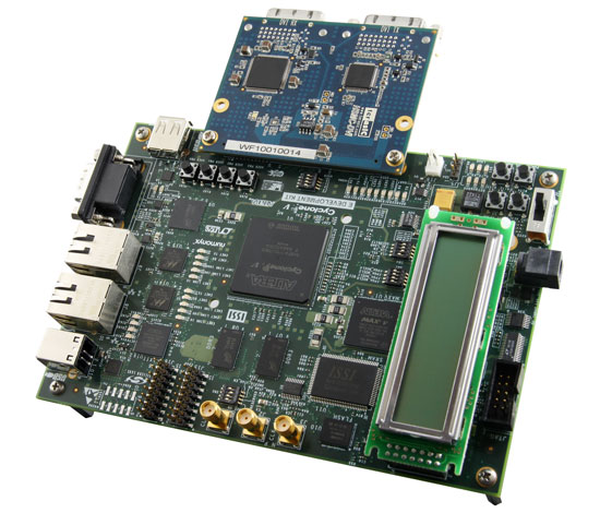
Cyclone V E Video Development System 
 
°¡    °Ý : °ßÀû¹®ÀÇ
Áß    ·® : 100g

Cyclone V E Video Development System

The Cyclone V E Video Development System is an ideal video processing platform for high-performance, cost-effective video applications. The Cyclone¢ç V E Development Kit offers a comprehensive general purpose development platform for many markets and applications. With multiple banks of DDR3 and LPDDR2 memory, this kit provides the ideal low-cost platform for high-bandwidth video processing. Additional features include an LCD character display, LEDs, user switches, USB and RJ-45 connectors.

The DVI-HSMC daughter card part of the bundled package will allow developers to access high quality and high resolution video signals that can support resolution up to 1600x1200. A complete DVI video controller design with source code is provided.

Terasic recognized for its strong design expertise in high-end video, imaging and multimedia products have made available a video development package that targets video processing development. The platform can also allow users to experience advanced image processing designs incorporating VIP (Altera¡¯s Video and Image Processing Suite MegaCore Functions).


Altera Cyclone V E Video Development System

Featured devices:

  • Cyclone V E FPGA - 5CEFA7F31C7NES
  • MAX V CPLD - 5M2210ZF256I5N (system controller)
  • MAX II CPLD - EPM240M100I5N (embedded USB Blaster II)

Configuration:

  • On-board USB-BlasterTM II cable (USB, PHY, Max¢ç V CPLD)
  • JTAG direct via JTAG header

Memory devices

  • DDR3 x32 at 300 MHz (soft memory controller)
  • LPDDR2 x16 (soft memory controller)
  • Flash (512 Mb)
  • SSRAM (18 Mb)
  • EEPROM (64 Kb)

General user input/output

  • User control
  • Four pushbuttons
  • Five LEDs
  • Four DIP switches
  • 2x Resets (CPU reset, Dev Clear)
  • LCD: Character LCD (16x2)

Components and interfaces

  • RJ45 for Ethernet
  • UART interface

Quartus¢ç II design software information

  • Quartus II Web Edition Software

Altera Cyclone V E FPGA Development Board Block Diagram

Terasic DVI-HSMC Card

Digital Transmitter

  • One DVI transmitter with single transmitting port
  • Digital Visual Interface (DVI) Compliant
  • Supports resolutions from VGA to UXGA (25 MHz – 165 MHz Pixel Rates)
  • Universal Graphics Controller Interface
    • 12-Bit, Dual-Edge and 24-Bit, Single-Edge Input Modes
    • Adjustable 1.1 V to 1.8 V and Standard 3.3 V CMOS Input Signal Levels
    • Fully Differential and Single-Ended Input Clocking Modes
    • Standard Intel 12-Bit Digital Video Port Compatible as on Intel¢â 81x Chipsets
  • Enhanced PLL Noise Immunity
    • On-Chip Regulators and Bypass Capacitors for Reducing System Costs
  • Enhanced Jitter Performance
    • No HSYNC Jitter Anomaly
    • Negligible Data-Dependent Jitter
      • Programmable Using I©÷C Serial Interface
      • Single 3.3-V Supply Operation

Digital Receiver

  • One DVI receiver with single receiving port
  • Supports UXGA Resolution (Output Pixel Rates Up to 165 MHz)
  • Digital Visual Interface (DVI) Specification Compliant
  • True-Color, 24 Bit/Pixel, 16.7M Colors at 1 or 2-Pixels Per Clock
  • Laser Trimmed Internal termination Resistors for Optimum Fixed Impedance Matching
  • 4x Over-Sampling
  • Reduced Ground Bounce Using Time Staggered Pixel Outputs
  • Lowest Noise and Best Power Dissipation Using TI PowerPAD¢â Packaging
Layout

Documents

TitleVersionSize(KB)Date AddedDownload
Cyclone V E FPGA Development Kit User Guide (PDF) 2013-01-08
Cyclone V E FPGA Development Board Reference Manual (PDF) 2013-01-08

CD-ROM

TitleVersionSize(KB)Date AddedDownload
DVI Combo CD-ROM 2013-02-01
Kit installation 2013-01-08


»óÈ£¸í
: (ÁÖ)¿ì¸²Æ¼¾Ø¾ÆÀÌ   ´ëÇ¥ÀÚ¸í : ±è¼®¹ü   »ç¾÷ÀÚµî·Ï¹øÈ£ : 211-87-88913  À̸ÞÀÏ : jun@woorimtni.co.kr
º»»ç : ¼­¿ï °­³²±¸ ºÀÀº»ç·Î 129 °ÅÆòŸ¿î 1204È£ ´ëÇ¥ÀüÈ­ : 82-2-512-7661  Æѽº : 82-2-512-7662
Copyright(C) 2011 Woorimtni Technologies All Rights Reserved.