Academic 가격 견적은 전화로 문의주시기 바랍니다.
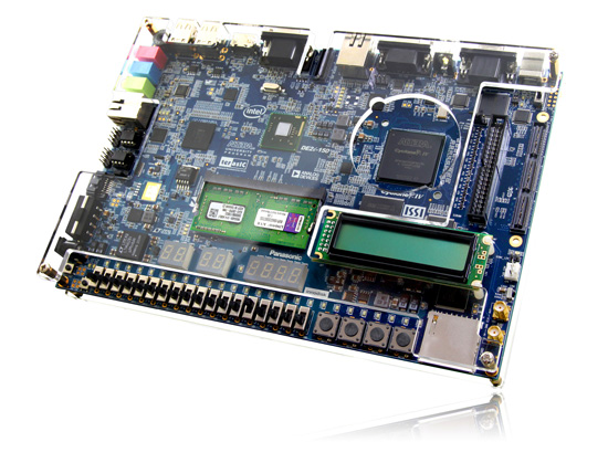
A groundbreaking embedded platform that combines an Intel embedded N2600 processor with the flexibility of
an Altera Cyclone IV GX FPGA, DE2i-150 is a full-featured computer system that fuses together the world
of high performance processing and unbelievably high configurability. The Altera Cyclone IV GX FPGA on the DE2i-150
board is able speed up the responsiveness of the system while still keeping your solution cost and power effective.
DE2i-150 is equipped with around 150K logic elements with ultimate flexibility in terms of reconfiguration of
actual hardware circuity and intellectual property as well as on-board multimedia peripherals, extendibility
options for a true system-ready solution for any task.
The Intel Atom processor and the FPGA device are linked together via two high-speed PCIe lanes such that high speed communication between them is guaranteed. DE2i-150 offers a powerful hardware-software co-development environment with amazing and unlimited potential.
Microprocessor
CPU : Intel® Atom™ Dual Core Processor N2600( 1M Cache, 1.6GHz )
Intel® Hyper-Threading Technology( 4 exection threads )
Intel SpeedStep® Technology
Instruction Set : 64-bit
Instruction Set Extensions : SSE2, SSE3, SSSE3
Integrated Graphics
Graphics Base Frequency : 400MHz
Chipset : Intel® NM10 Express Chipset
DMI x2 to CPU
Intel® High Definition Audio
Serial ATA (SATA) 3 Gb/s
Universal Serial Bus(USB) Hi-Speed USB 2.0
PCI Express Gen 1
Memory
DDR3 SO-DIMM SDRAM
Ethernet
Intel® 82583V GbE Controller
10/100/1000 Mb/s RJ45
3 status indicting LEDs
Display
VGA
HDMI 1.3a
Audio Codec
Realtek ALC272VA3-GR
Bios
DIP package Bios Flash : GD25Q16
Programming Interface for Bios : Dedi-Prog Interface
Debug Interface
XDP header
Clock System
CK505 : 9VRS4339B
32768 Hz RTC crystal
27MHz VGA clock source
Others
Power header for hard-disk
Current limit for USB
Buzzer
Mini PCIE header (Default for Intel® Centrino® Advance-N 6205 WiFi module)
mSATA header
RTC battery : CR2032
FPGA
Featured devices
Cyclone IV GXP4CGX150F31 device
149,760 LEs
720 M9K memory blocks
6,480 Kbits embedded memory
8 PLLs
FPGA configuration
JTAG and AS mode configuration
EPCS64 serial configuration device
On-board USB Blaster circuitry
Memory devices
128MB (32Mx32bit) SDRAM
4MB (1Mx32) SSRAM
64MB (4Mx16) Flash with 16-bit mode
SD Card socket
Provides SPI and 4-bit SD mode for SD Card access
Connectors
Ethernet 10/100/1000 Mbps ports
High Speed Mezzanine Card (HSMC)
40-pin expansion port
VGA-out connector
VGA DAC (high speed triple DACs)
DB9 serial connector for RS-232 port with flow control
Clock
Three 50MHz oscillator clock inputs
SMA connectors (external clock input/output)
Display
16x2 LCD module
Switches and indicators
18 slide switches and 4 push-buttons switches
18 red and 9 green LEDs
Eight 7-segment displays
Other features
Infrared remote-control receiver module
TV decoder (NTSC/PAL/SECAM) and TV-in connector
Block Diagram
Documents
| DE2i-150 Getting Started Guide |
1.0 |
1397 |
2013-06-14 |
 |
| DE2i-150 FPGA System User Manual |
1.2 |
7131 |
2013-06-14 |
 |
| DE2i-150 Quick Start Guide |
1.2 |
1301 |
2013-06-14 |
 |
| My First FPGA |
1.0 |
2114 |
2013-06-14 |
 |
| My First NiosII |
1.0 |
5452 |
2013-06-14 |
 |
BIOS
| DE2i-150 BIOS |
58 |
|
2013-07-24 |
 |
CD-ROM
| DE2i-150 CD-ROM |
- |
|
2013-06-14 |
 |
Please note that all the source codes are provided "as is". For further support or modification, please contact Terasic Support and your request will be transferred to Terasic Design Service.More resources about IP and Dev. Kit are available on Altera User Forums. |
