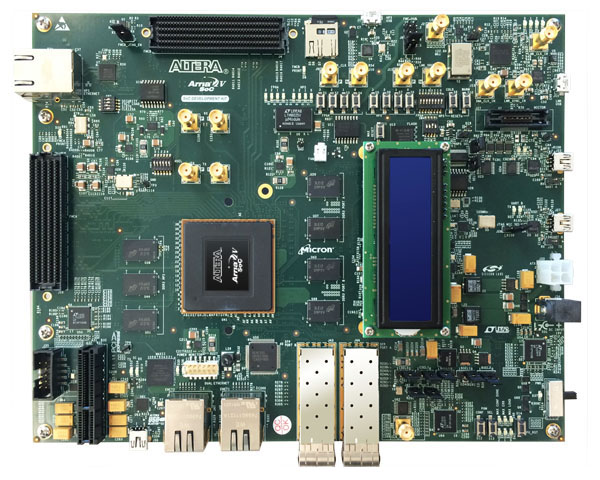
The Altera® Arria® V SoC Development Kit offers a quick and simple approach to develop custom ARM® processor-based SoC designs. Altera’s midrange, transceiver-based Arria V FPGA fabric provides the highest bandwidth with the lowest total power for midrange applications such as:
- Remote radio units*
- 10G/40G line cards*
- Medical imaging
- Broadcast studio equipment.
- Acceleration of image- and video-processing applications*
- PCI Express® (PCIe®) Gen2 x4 lanes (endpoint or rootport)
*Application-specific daughtercards, available separately, supporting a wide range of I/O and interface standards.
Featured devices
- Arria V ST SoC—5ASTFD5K3F40I3NES (SoC)
- MAX® V CPLD—5M2210ZF256C4N (system controller)
- MAX II CPLD—EPM570GF100 (embedded USB-BlasterTM II cable)
FPGA configuration sources
- Embedded USB-Blaster II (JTAG) cable
- EPCQ flash (Active Serial x1 or x4 configuration)
- Flash fast passive parallel (FPP)
- Hard processor system (HPS)
FPGA memory
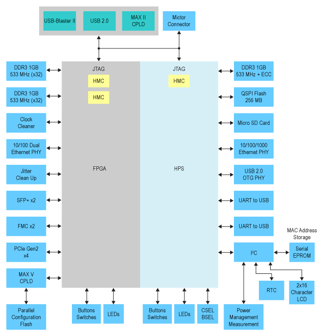
- 2x 1,024 MB 32-bit DDR3 SDRAM
- 1x 512 Megabit (Mb) CFI synchronous Flash
- 1x 256 Mb NOR Flash (EPCQ)
FPGA I/O interfaces
- 1x PCI Express x4 Gen2 socket
- 2x FPGA mezzanine card (FMC) portds
- 2x 10/100 Ethernet ports
- 2x SPF+ ports
- 4x user LEDs
- 4x user pushbuttons
- 4x user dip switches
- HPS boot sources
- 512 Mb QSPI Flash
- Removable micro-SDCard flash
- FPGA
HPS memory
- 1x 1,024 Mbyte (MB) DDR3 SDRAM with ECC
- 1x 512 Mb QSPI flash
- Micro-SDCard socket with 4 GB micro-SDCard flash device
- One 32 Kb I2C serial EEROM
HPS I/O interfaces
- 1x 1 Gigabit Etherent port (HPS)
- 1x USB 2.0 on-the-go (OTG) port (HPS)
- 2x RS-232 UART (through mini-USB port)
- x1 real-time clock (with battery backup)
- x1 two-line text LCD
- x4 user LEDs
- x4 user push buttons
- x4 DIP switches
Clocking
- Four-output programmable clock generator for FPGA reference clock inputs
- 148.5 MHz LVDS programmable voltage-controlled crystal oscillator (VCXO) for FPGA reference clock input
- 50 MHz single-ended oscillator for FPGA and MAX V FPGA clock input
- 100 MHz single-ended oscillator for MAX V FPGA configuration clock input
- SMA inputs for FPGA and HPS clocks
- LMK04828 clock jitter cleaner
Power
- Laptop DC input 14—20 V adapter
System monitoring circuit
- Power (voltage, current, wattage)
Mechanical
- Board dimensions—7.175” x 9”

Documents
| Arria V SoC Development Kit User Guide | 1.0 | 3136 | 2014-06-04 |  |
| Arria V SoC Development Board Reference Manual | 1.0 | 1978 | 2014-06-04 |  |
CD-ROM
| Kit installation (EXE) (Windows) | 13.1.0.5 | | 2014-06-04 |  |
| Kit installation (ZIP) (Linux) | 13.1.0.5 | | 2014-06-04 |  |
Please note that all the source codes are provided "as is". For further support or modification, please contactTerasic Support and your request will be transferred to Terasic Design Service.More resources about IP and Dev. Kit are available on
Altera User Forums.
- Arria V ST FPGA Development Kit software content
- Design examples
- Complete documentation
- SoC Embedded Design Suite Subscription Edition
ARM Development Studio 5 (DS-5™) Altera Edition Toolkit
Hardware-to-software handoff tools
Linux run-time software for application development
SoC hardware libraries for firmware development
Application examples
- Free software supported by Quartus® II software v13.1, Subscription Edition
