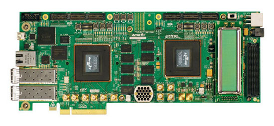
The Altera® Arria® V GT FPGA Development Kit provides a complete design environment that includes all the hardware and software that you need to develop full FPGA designs and test them within a system environment. The development kit is RoHS compliant, and includes the following features:
- Two FPGAs for system-level design
- Arria V GT FPGA: 504K logic elements (LEs), F1517 package, 36 6G tranceivers, and I3 speed grade
- Three I/O expansion slots: two high-speed mezzanine cards (HSMCs) and one FPGA mezzanine card (FMC)
- 2 GB of DDR3 SDRAM memory, 4.5 MB of QDR II+ memory, and 1 Gb of flash memory
- Two SFP+ connections
- SMAs and the new Samtec Bull's Eye connectors
- Ability to measure individual power rails on each chip
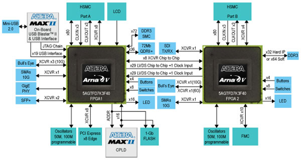
Unit 1: Arria V GT FPGA: 5AGTD7K3F40I3N
- Memory
- 1,152-MB x72 DDR3 SDRAM
- 4.5-MB (1 Mb x 36) QDR II+ SRAM
- 1-Gb sync flash (x16)
- Communication ports
- PCI Express® (PCIe® ) x8 edge connector
- HSMC Port A (Eight transceiver channels)
- USB 2.0
- Gbps Ethernet
- Chip-to-chip bridge with 29 LVDS inputs and 29 LVDS outputs, and x8 transceivers
- Two SFP+ channel
- Bull's Eye connector (Three 10-Gbps transceiver channel)
- SMA connector (One 10-Gbps transceiver channel)
- Configuration
- JTAG
- Fast passive parallel (FPP) parallel flash loader (PFL)
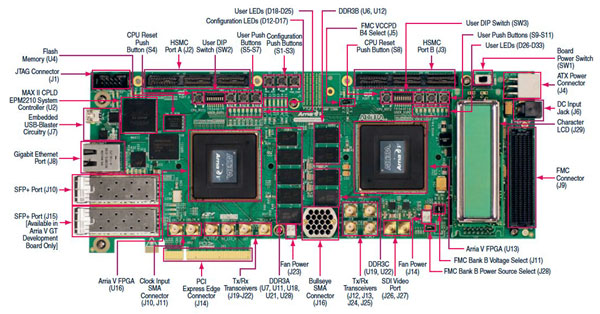
- Buttons, switches, LEDs, and displays
- One CPU reset push button
- Three user push buttons
- Eight dual in-line package (DIP) switches
- 16 user LEDs (eight bi-color diodes)
- Three PCIe LEDs
- Three HSMA Status LEDs
- 16x2 character LCD
Unit 2: Arria V GT FPGA: 5AGTD7K3F40I3N
- Memory
- x64 DDR3 SDRAM soft controller (or x32 hard intellectual property (IP) controller)
- Communication ports
- HSMC Port B (Four transceiver channels)
- FMC Port (Ten transceiver channels)
- Chip-to-chip bridge with 29 LVDS inputs and 29 LVDS outputs, and x8 transceivers
- One serial digital interface (SDI) channel
- Bull's Eye connector (One 6-Gbps transceiver channel)
- Bull's Eye connector (One 10-Gbps transceiver channel)
- SMA connector (One 10-Gbps transceiver channel)
- Configuration
- Buttons, switches, LEDs, and displays
- One CPU reset push button
- Three user push buttons
- Eight DIP switches
- 16 user LEDs (eight bi-color diodes)
Miscellaneous
- EPM2210GF324 system controller
- EPM570GM100 on-board USB-Blaster™ II download cable
Clocking
- 50 MHz and 148.5-MHz oscillator
- 100 MHz and four 4 output programmable oscillators
- SMA input (LVPECL)
Power
- Laptop DC input
- PCIe edge connector
System monitoring
- Power (voltage, current, and wattage)—per unit per rail
Arria V GT FPGA Development Board Block Diagram
Documents
| Arria V GT FPGA Development Board Reference Manual (PDF) | | | 2013-01-07 |  |
| Arria V GT FPGA Development Kit User Guide (PDF) | | | 2013-01-07 | |
CD-ROM
| Kit installation | | | 2013-01-07 |  |
Please note that all the source codes are provided "as is". For further support or modification, please contactTerasic Support and your request will be transferred to Terasic Design Service.More resources about IP and Dev. Kit are available on
Altera User Forums.
- Loopback and debug HSMC cards
- Samtec's Bull's Eye assembly kit
- Power adapter and cables
- Arria V GT FPGA Development Kit software content
- Complete documentation
- User guide
- Reference manual
- Board schematics and layout design files
- GUI-based Board Test System
- Includes complete Quartus II software projects with open source register transfer level (RTL)
- Board Update Portal
- Includes complete Quartus II software projects with open source RTL
- Quartus II design software, Development Kit Edition (DKE)


