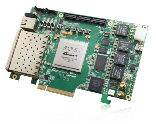
The Terasic TR5-F40W Stratix V GX FPGA Development Kit provides the ideal hardware platform for developing high-performance and high-bandwidth application. With a standard-height, half-length form-factor package, the TR5-F40W is designed for the most demanding high-end applications, empowered with the top-of-the-line Altera Stratix V GX, delivering the best system-level integration and flexibility in the industry.
The Stratix® V GX FPGA features 340K logic elements and integrated transceivers that transfer at a maximum of 12.5 Gbps, allowing the TR5-F40W to be fully compliant with version 3.0 of SATA, version 3.0 of the PCI Express standard, as well as allowing an ultra low-latency, straight connections to four external 10G SFP+ modules. Not relying on an external PHY will accelerate mainstream development of network applications enabling customers to deploy designs for a broad range of high-speed connectivity applications. An HSMC expansion port also allows users to connect custom daughter cards such as those found on cards.terasic.com. The feature-set of the TR5-F40W fully supports all high-intensity applications such as low-latency trading, cloud computing, high-performance computing, data acquisition, network processing, and signal processing.
* Memory Solution for Altera FPGAs 
| * Power Solution for Altera FPGAs

| * Flash Solution for Altera FPGAs

|
| | | |
*USB solution for Altera FPGAs 
| *Clock and Voltage Translation solution for Altera FPGAs 
| * Passive Component Solution for Altera FPGAs 
|
The TR5-F40W Board
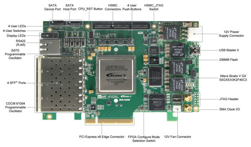
Altera Stratix® V GX FPGA (5SGXEA3K2F40C3)
- On-Board USB Blaster II or JTAG header for FPGA programming
- Fast passive parallel (FPPx32) configuration via MAX II CPLD and flash memory
General user input / output:
- 4 LEDs
- 1 LED Array
- 4 push-buttons
- 4 slide switches
On-Board Clock
- 50MHz Oscillator
- Programmable oscillators Si570 and CDCM61004
Memory
Communication Ports
- Four SFP+ connectors
- One SATA host port
- One SATA device port
- PCI Express (PCIe) x8 edge connector
- One RS422 transceiver with RJ45 connector
- One HSMC Connector (voltage levels: 2.5/1.8/1.5V)
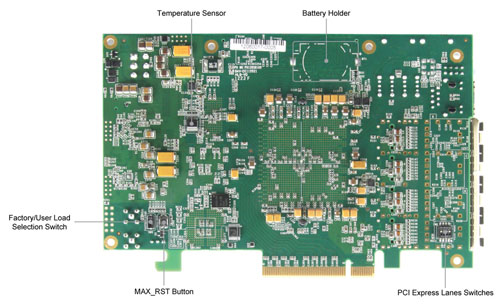
System Monitor and Control
- Temperature sensor
- Fan control
Power
- PCI Express 6-pin power connector, 12V DC Input
- PCI Express edge connector power
Mechanical Specification
- PCI Express standard height and half-length
Documents
| TR5-F40W User Manual | | 7217 | 2014-09-01 |  |
CD-ROM
| TR5-F40W CD-ROM (Using Quartus 14.0) | 1.1.1 | | 2014-10-31 |  |
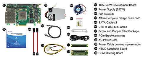
The TR5-F40W package includes:
Quartus design software license is not included in this kit.


