The Terasic TR5-F40W Stratix V GX FPGA Development Kit provides the ideal hardware platform for developing high-performance and high-bandwidth application. With a standard-height, half-length form-factor package, the TR5-F40W is designed for the most demanding high-end applications, empowered with the top-of-the-line Altera Stratix V GX, delivering the best system-level integration and flexibility in the industry.
The Stratix® V GX FPGA features 340K logic elements and integrated transceivers that transfer at a maximum of 12.5 Gbps, allowing the TR5-F40W to be fully compliant with version 3.0 of SATA, version 3.0 of the PCI Express standard, as well as allowing an ultra low-latency, straight connections to four external 10G SFP+ modules. Not relying on an external PHY will accelerate mainstream development of network applications enabling customers to deploy designs for a broad range of high-speed connectivity applications. An HSMC expansion port also allows users to connect custom daughter cards such as those found on cards.terasic.com. The feature-set of the TR5-F40W fully supports all high-intensity applications such as low-latency trading, cloud computing, high-performance computing, data acquisition, network processing, and signal processing.
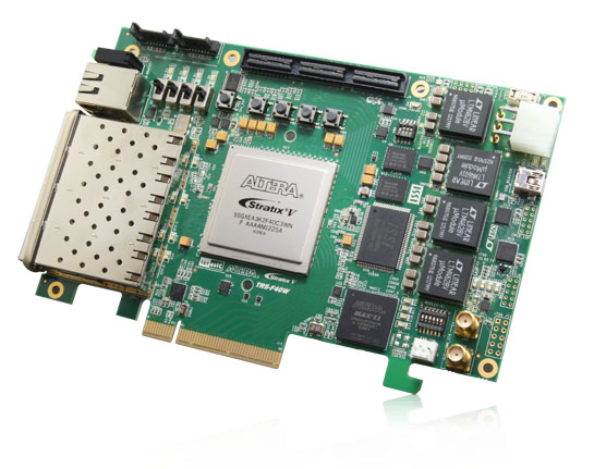
The TR5-F40W Board
Altera Stratix® V GX FPGA (5SGXEA3K2F40C3)
- On-Board USB Blaster II or JTAG header for FPGA programming
- Fast passive parallel (FPPx32) configuration via MAX II CPLD and flash memory
General user input / output:
- 4 LEDs
- 1 LED Array
- 4 push-buttons
- 4 slide switches
On-Board Clock
- 50MHz Oscillator
- Programmable oscillators Si570 and CDCM61004
Memory
Communication Ports
- Four SFP+ connectors
- One SATA host port
- One SATA device port
- PCI Express (PCIe) x8 edge connector
- One RS422 transceiver with RJ45 connector
- One HSMC Connector
System Monitor and Control
- Temperature sensor
- Fan control
Power
- PCI Express 6-pin power connector, 12V DC Input
- PCI Express edge connector power
Mechanical Specification
- PCI Express standard height and half-length
Download
Documents
| TR5-F40W User Manual | | 7217 | 2014-09-01 |  |
CD-ROM
| TR5-F40W CD-ROM (Using Quartus 14.0) | 1.1.0 | | 2014-09-01 |  |
Please note that all the source codes are provided "as is". For further support or modification, please contactTerasic Support and your request will be transferred to Terasic Design Service.More resources about IP and Dev. Kit are available on
Altera User Forums.
The TR5-F40W package includes:


