|
|
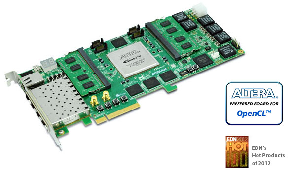
The Terasic DE5-Net Stratix V GX FPGA Development Kit provides the ideal hardware solution for designs that demand high capacity and bandwidth memory interfacing, ultra-low latency communication, and power efficiency. With a full-height, 3/4-length form-factor package, the DE5-Net is designed for the most demanding high-end applications, empowered with the top-of-the-line Altera Stratix V GX, delivering the best system-level integration and flexibility in the industry. The Stratix® V GX FPGA features integrated transceivers that transfer at a maximum of 12.5 Gbps, allowing the DE5-Net to be fully compliant with version 3.0 of the PCI Express standard, as well as allowing an ultra low-latency, straight connections to four external 10G SFP+ modules. Not relying on an external PHY will accelerate mainstream development of network applications enabling customers to deploy designs for a broad range of high-speed connectivity applications. For designs that demand high capacity and high speed for memory and storage, the DE5-Net delivers with two independent banks of DDR3 SO-DIMM RAM, four independent banks of Cypress QDRII+ SRAM or functional compatible SRAMS provided by GSI and ISSI, high-speed parallel flash memory, and four SATA ports. The feature-set of the DE5-Net fully supports all high-intensity applications such as low-latency trading, cloud computing, high-performance computing, data acquisition, network processing, and signal processing. * Cypress QDRII+ SRAM or functional compatible SRAMs
 IS61QDPB44M18A1-450M3LI IS61QDPB44M18A1-450M3LI
 GS8662DT20BGD-550 GS8662DT20BGD-550
 CY7C25632KV18-500BZXI CY7C25632KV18-500BZXI * Power Solution for Altera FPGAs
 * Passive Component Solution for Altera FPGAs
 * X2Y Power Decoupling Solution 
FPGA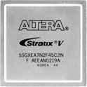 | FPGA Altera Stratix® V GX FPGA (5SGXEA7N2F45C2) FPGA Configuration On-Board USB Blaster II or JTAG header for FPGA programming Fast passive parallel (FPPx32) configuration via MAX II CPLD and flash memory |
Memory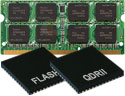 | Memory Up to 8GB DDR3 800 MHz SO-DIMM SDRAM 32MB SRAM (ISSI QUADP for DE5-Net 450, GSI SigmaQuad-II+ for DE5-Net 550, Cypress QDRII+ for DE5-Net 500) 256MB FLASH |
Communication | Communication Ports Four SFP+ connectors Two Serial ATA host ports Two Serial ATA device ports PCI Express (PCIe) x8 edge connector (includes Windows x32-bits/64-bits PCIe drivers) One RS422 transceiver with RJ45 connector |
Others | General user input / output: 4 LEDs 1 LED Array 4 push-buttons 4 slide switches 2 seven-segment displays SMA clock input / output On-Board Clock 50MHz Oscillator Programmable oscillators Si570, CDCM61001 and CDCM61004 System Monitor and Control Temperature sensor Fan control Power PCI Express 6-pin power connector, 12V DC Input PCI Express edge connector power Mechanical Specification PCI Express standard height and 3/4-length PCI Express edge connector power |
Block Diagram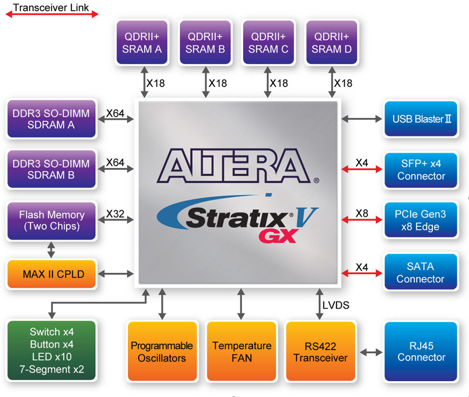
DownloadOpenCL BSP(Board Support Package)| OpenCL User Manual | - | 2.93MB | 2014-07-07 |  | | DE5NET_openCL_BSP(.zip) | 3.12 | 136MB | 2014-02-07 |  | | DE5NET_openCL_BSP(.tar.bz2) | 3.12 | 136MB | 2014-02-07 | |
Document| DE5-Net User Manual | 1.11 | 6215 | 2012-11-20 |  |
CD-ROM| DE5-Net System CD | 1.2.0 | | 2014-04-25 |  |
Please note that all the source codes are provided "as is". For further support or modification, please contactTerasic Support and your request will be transferred to Terasic Design Service.More resources about IP and Dev. Kit are available on Altera User Forums. DE5-Net Tools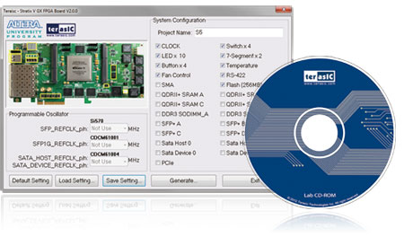
System BuilderThe System Builder allows users to create a Quartus II project that includes the top-level design file, pin assignments, and I/O standard setting for the board. Reference DesignsThe FPGA System CD Kit contains various reference designs with source code and complete document reducing the development cycle. - DDR3 SDRAM Test
- SigmaQuad-II+/QDRII+/QUADP Test
- PCIe Express Communication
- Programmable Oscillator
|
|
|


