Altera's 100G Development Kit, Stratix® V GX Edition enables a thorough evaluation of 100G designs by allowing you to:
- Support 10G/40G and 100G line interfaces through optical modules
- Support applications requiring external memory interfaces, through 6x32-bit DDR3 and 1x36- and 1x18-bit QDRII BL2 memory banks
- Use system-side interfaces via two pairs of FCI AirMax connectors
- Complete line-side (optical modules) to system-side (AirMax connector) datapath analysis
- Evaluate transceiver performance up to 12.5 Gbps
- Verify physical medium attachment (PMA) compliance to 10G/40G/100G Ethernet, Interlaken, CEI-6G/11G, and other major standards
- Validate interoperability between optical modules, such as SFP, SFP+, QSFP, and CFP
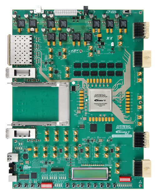
Stratix V GX development board
- Featured device: 5SGXEA7N2F45C2N
- EPM2210F324C3N, MAX® II 324-pin CPLD
FPGA configuration
- Fast Passive Parallel (FPP) configuration
- 1-Gb flash storage for two configuration images (factory and user)
- On-board USB-Blaster™ II cable for use with the Quartus® II Programmer, Nios® II software and System Console
- JTAG header for external USB-Blaster cable
Memory
- Twelve 2-Gb DDR3 SDRAM
- Two 72-Mb QDR II SRAM
General user input/output
- Four user push buttons
- Two DIP switches
- Eight user LEDs
- Two-line character LCD
- Ten configuration status LEDs
Components and interfaces
- 10/100/1000 Ethernet PHY and RJ-45 jack
- 48 transceiver channels
- Two channels for SMA interface
- Four channels for SFP+ interface
- Eight channels for QSFP interface
- 10 channels for CFP interface
- 24 channels for Interlaken interface
Temperature measurement circuitry
Power
- 19-V DC input
- 2.5-mm barrel jack for DC power input
- On/off power slide switch
- On-board power measurement circuitry
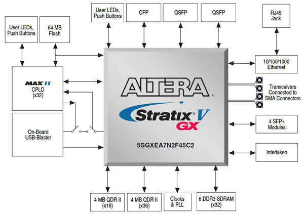
Altera 100G Development Kit, Stratix V GX Edition Block Diagram
Documents
| User Guide (PDF) | 11.1 | | 2013-01-04 |  |
| Reference Manual (PDF) | | | 2013-01-04 | |
CD-ROM
| Kit Installation | 12.0 | | 2013-01-04 |  |
Please note that all the source codes are provided "as is". For further support or modification, please contactTerasic Support and your request will be transferred to Terasic Design Service.More resources about IP and Dev. Kit are available on
Altera User Forums.


