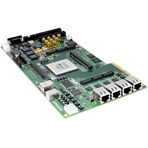
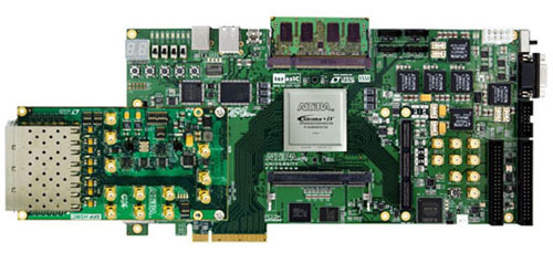
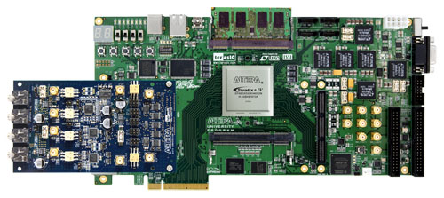
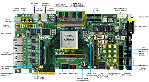
The DE4 Development Board provides the ideal hardware platform for system designs that demand high-performance, serial connectivity, and advanced memory interfacing. Developed specifically to address the rapidly evolving requirements in many end markets for greater bandwidth, improved jitter performance, and lower power consumption. The DE4 is powered by the Stratix® IV GX device and supported by industry-standard peripherals, connectors and interfaces that offer a rich set of features that is suitable for a wide range of compute-intensive applications. The evaluation of transceiver performance for jitter, protocol compliance, and equalization on the DE4, exceeded the Stratix IV GX performance standard with transceivers operating at 10 Gbps on SATA and HSMC interfaces!
The advantages of the Stratix® IV GX FPGA platform with embedded transceivers has allowed the DE4 to fully compliant with version 2.0 of the PCI Express standard in addition to serial ATA (SATA) interfaces making it possible to leverage the integration option for storage applications. The DE4 delivers fully tested and supported connectivity targeted reference design that integrates built-in blocks for PCI Express, SATA transceivers, and Gigabit Ethernet protocol. Situated on the DE4 also includes two DDR2 SO-DIMM socket supporting maximum capacity of 8-Gbyte of volatile memory for user applications which are capable running at 400 MHz clock rate.
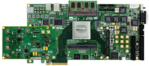
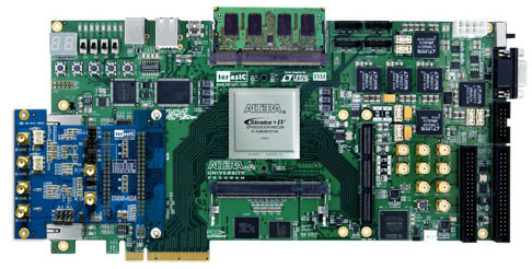
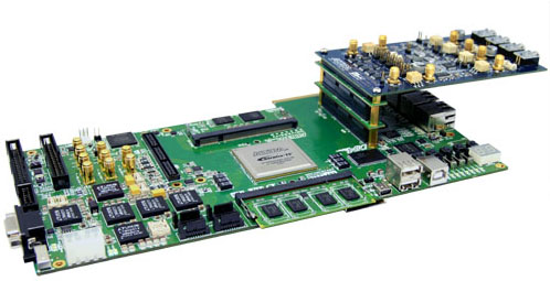
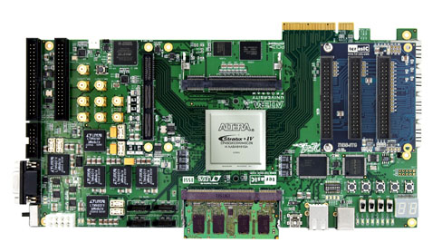
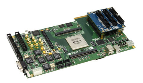
The DE4 is supported by multiple targeted reference designs and two High-Speed Mezzanine Card (HSMC) connectors that allow scaling and customization with mezzanine daughter cards. For large-scale ASIC prototype development, it can be established by a cable connecting to multiple DE4/FPGA boards through the HSMC connectors.
* Power Solution for Altera FPGAs
* Memory Solution for Altera FPGAs

* X2Y Power Decoupling Solution

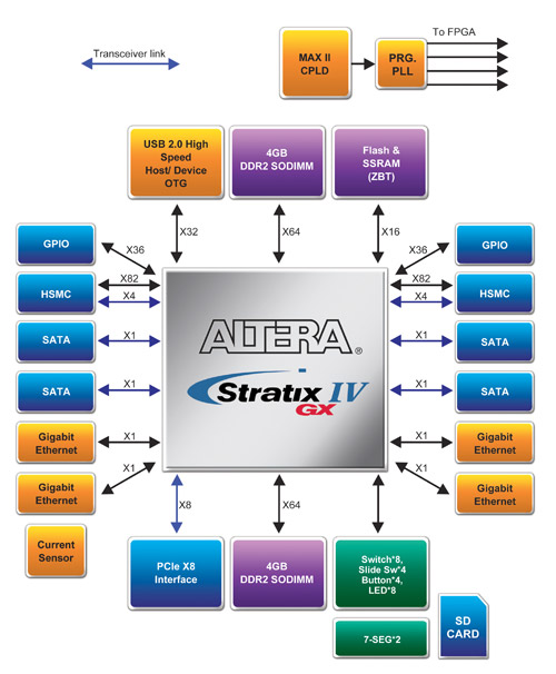
Stratix IV GX EP4SGX230
- 228,000 logic elements (LEs)
- 17,133K total memory Kbits
- 1,288 18x18-bit multipliers blocks
- 2 PCI Express hard IP blocks
- 744 user I/Os
- 8 phase locked loops (PLLs)
Stratix IV GX EP4SGX530
- 531,200 logic elements (LEs)
- 27,376K total memory Kbits
- 1,024 18x18-bit multipliers blocks
- 4 PCI Express hard IP Blocks
- 744 user I/Os
- 8 phase locked loops (PLLs)
FPGA Configuration
- JTAG and Fast Passive Parallel (FPP) configuration
- On-board USB Blaster
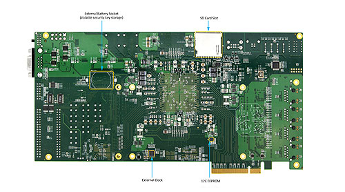
Memory Devices
- 64 MB Flash with a 16-bit data bus
- 2 MB ZBT SSRAM
- I2C EEPROM
Two DDR2 SO-DIMM Sockets
- 400 MHz clock rate
- Maximum theoretical bandwidth of over 102 Gbps
- Up to 8-Gbyte capacity in total
SD Card Socket
- Provides SPI and 4-bit SD mode for SD Card access
Buttons, Switches and LEDs
- 4 push-buttons
- 4 slide switches
- 8 LEDs
- 8-position DIP switch
Two Seven Segments
- Two independent seven segments
On-Board Clocks
- 3 Programmable PLLs configured via FPGA
- o HSMA, HSMB transceiver clock source
- o SATA reference clock
- o FPGA LVDS clock input
- 50MHz/100MHz oscillator
SMA Connectors
- 2 SMA connector for external transceiver clock input
- 4 SMA connector for LVDS clock input/output
- 2 SMA connectors for clock output
- 1 SMA connector for external clock input
Four Serial ATA Ports
- Support SATA 3.0 standard 6Gbps signaling rate
- Two host and two device ports
Four Gigabit Ethernet Ports
- Integrated 1.25 GHz SERDES
PCI Express x8 Edge Connector
- Support connection speed of Gen1 at 2.5Gbps/lane to Gen2 at 5.0Gbps/lane
- Connection established with PC motherboard with x8 or x16 PCI Express slot
Two 172-pins High Speed Mezzanine Card (HSMC)
- 2 female-HSMC connectors
- I/O voltage 2.5V
- Total of 12 high-speed transceivers at 8.5 Gbps
- Total of 38 LVDS pair at 1.6 Gbps
Two 40-pin Expansion Headers
- 72 FPGA I/O pins, as well as 4 power and ground lines, are brought out to two 40-pin expansion connectors
- 40-pin header is designed to accept a standard 40-pin ribbon cable used for IDE hard drives
- I/O voltage 3.0V
USB Host/Slave Controller
- Complies fully with Universal Serial Bus Specification Rev. 2.0
- Support data transfer at high-speed, full-speed, and low-speed
- Support both USB host and device
- Three USB ports (one type mini-AB for host/device and two type A for host)
- Support Programmed I/O (PIO) and Direct Memory Access (DMA)
Power
- DC input 12V and 3.3V
- PCI Express edge connector power
- Support PCI Express external standard power source
- On-Board power measurement circuitry
Block Diagram
 Connect MTL
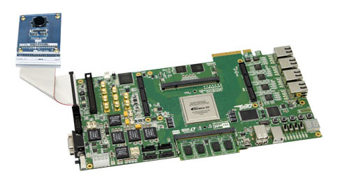
Connect D5M
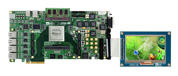
Connect LTM
Connect DVI-HSMC
Connect SFP-HSMC
Connect SDI-HSMC
Connect ADA-HSMC
Connect DCC-HSMC
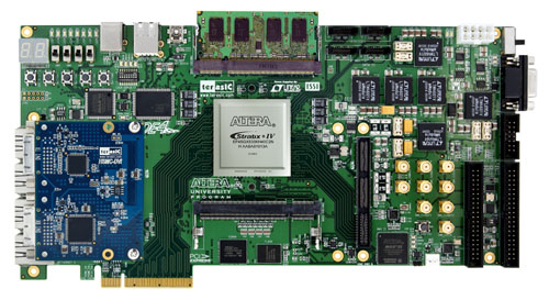
Connect HTG
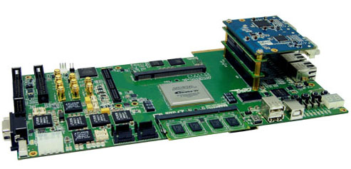
Connect COMM
Connect MSV
Download
Documents
| DE4 User Manual | | 13984 | 2010-08-23 |  |
CD-ROM
| DE4 CD-ROM | 1.3.0 | | 2014-04-30 |  |
| PCIe Driver and Applicaiton Software (Windows7/XP x 64-bits/32-bits) | | | 2012-04-10 | |
Please note that all the source codes are provided "as is". For further support or modification, please contactTerasic Support and your request will be transferred to Terasic Design Service.More resources about IP and Dev. Kit are available on
Altera User Forums.
DE4 Tools
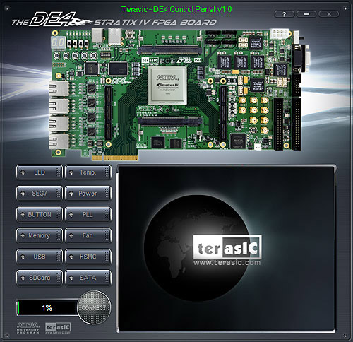
DE4 Control Panel – allows users to access various components on the DE4 board from a host computer.
DE4 Control Panel
DE4 System Builder – a powerful tool comes with the DE4 board. This tool will allow users to create a Quartus II project file on their custom design for the DE4 board. The top-level design file, pin assignments, and I/O standard settings for the DE4 board will be generated automatically by the DE4 System Builder. In addition, through the HSMC connectors you can select various daughter cards in conjunction with the DE4 using the DE4 System Builder.
DE4 System Builder
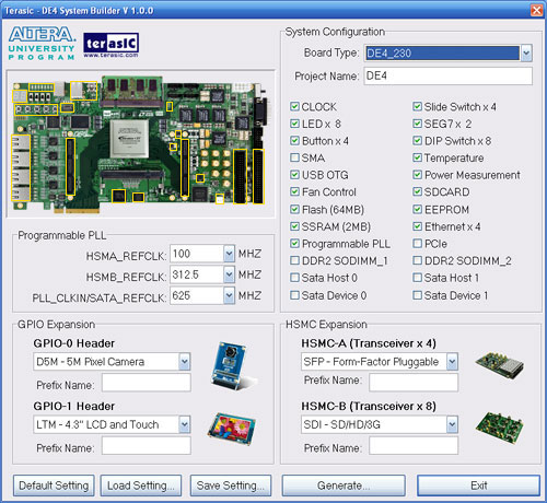
The generated Quartus II project files include the following:
- Quartus II Project File (.qpf)
- Quartus II Setting File (.qsf)
- Top-Level Design File (.v)
- External PLL Contorller (.v)
- Synopsis Design Constraints file (.sdc)
- Pin Assignment Document (.htm)
DE4 Demonstrations
Reference Designs
- USB Host
- USB Device
- Ethernet – Simple Socket Server
- PCIe Simple I/O Control
- PCIe Image Process Application
- Power Measurement
- SATA Loopback
- HSMC Loopback
- SD Card Reader
- PLL IP Configuration
- DDR2 SDRAM
- Web Server
The DE4 package includes:


