|
|
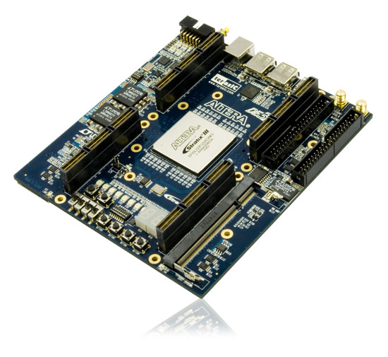
DE3-150 / DE3-260 / DE3-340 Special Price : $1,795 / $2,395 / $3,395 (starts from 06/11/2012)
The Altera DE3 ASIC prototyping development board allows researchers and engineers to access the high density and high performance FPGA - the Altera Stratix III. Starting with the Stratix III 3SL150 (142K logic elements), the DE3 is the perfect platform for creating your cutting edge design in programmable logic. The DE3-150 board can be stacked up to create a programmable fabric that is unequaled by any other board system in the world. DE3 boards include the DE3-340 (338K logic elements) and the DE3-260 (254.4K logic elements) that are optimized with extra on-chip multipliers needed for DSP research and development. All of the DE3s can be stacked and all share the same set of function from the Terasic's daughter cards connected to them. Multiple DE3s can be joined together to increase design gate count and performance. FPGA Devices- Stratix III EP3SL150 (DE3-150)
- Stratix III EP3SE260 (DE3-260)
- Stratix III EP3SL340 (DE3-340)
- 338,000 logic elements (LEs)
- 16,272K total memory Kbits
- 576 18x18-bit multipliers blocks
- 736 user I/Os
The DE3 board has powerful features that allow the user to implement resource and time consuming designed circuits, specifically for high-speed application and projects with complex algorithms. - Built-in USB Blaster for programming and user API control
- JTAG programming mode
- DDR2 SO-DIMM socket
- 4 push-button switches
- 1 DIP switch ( x8)
- 4 slide switches
- 8 RGB LEDs
- 2 seven-segment displays
- USB Host/Slave Controller with one mini-AB for host/device and two type A for device
- SD Card socket
- 50MHz onboard oscillator for clock source
- 1 SMA connector for external clock input
- 1 SMA connector for PLL clock output
- Eight 180-pin High Speed Terasic Connectors ( HSTC ), where 4 male and 4 female connectors are on the top and bottom of DE3, respectively.
- Two 40-pin Expansion Headers
High speed I/O performanceHigh Speed Samtec Cable: REF-136223-02 (QSH-090-01-F-D-A-K) High speed I/O performance: The live test shows that the highest speed I/O transmission reaches the ultimate 1.25 Gbps (the top limitation of Stratix III). 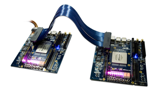
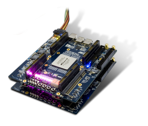
 MTL COMM MTL COMM 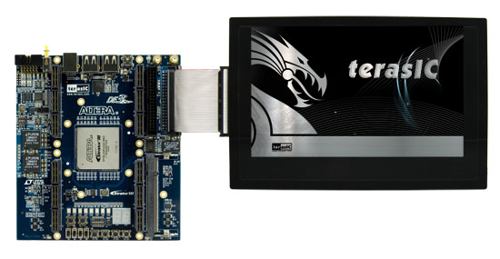
 Connect COMM Connect COMM DownloadDocuments
| DE3 User manual | | 6006 | 2009-11-09 |  |
CD-ROMReference Design- DE3 Control Panel
- USB device/host control demonstration
- SD Card access demonstration
- DDR2 SDRAM demonstration
System BuilderDE3 System Builder, a powerful tool comes with the DE3 board. This tool can help users to create the Quartus II project files for DE3 board basic on their custom design. The top-level design file, pin assignment, and I/O standard setting for the DE3 board will be generated automatically by the DE3 System Builder. The generated Quartus II project files include: - Quartus II Project File(.qpf)
- Quartus II Setting File(.qsf)
- Top-Level Deign File (.v)
- Synopsis Design Constraints file (.sdc)
- Encrypted Power Configuration Controller (.v)
- Pin Assignment Document (.htm)
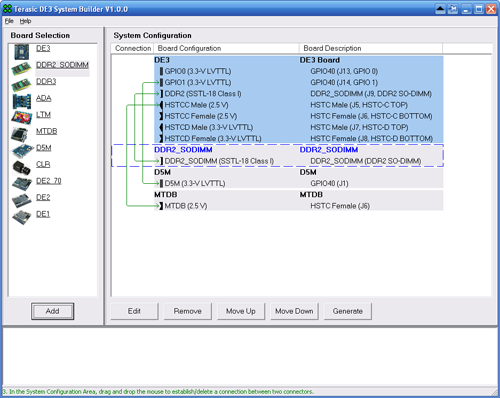
Control PanelThe DE3 board comes with a PC-based Control Panel that allows users to access various components on board. The host computer communicates with the board via USB port. The tool can be used to verify the functionality of components. 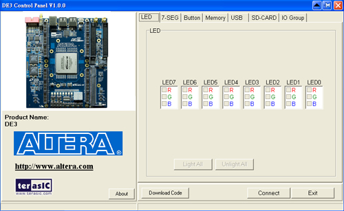
Customer Success with Terasic FPGA Platform Links to Universities using DE3 at classesSuccess Stories |
|
|
