|
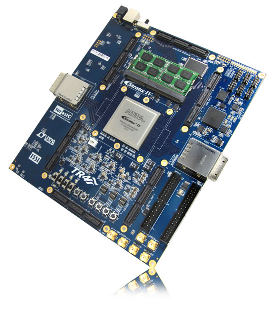
The TR4 Development Board provides the ideal hardware platform for system designs that demand high-performance, serial connectivity, and advanced memory interfacing. Developed specifically to address the rapidly evolving requirements in many end markets for greater bandwidth, improved jitter performance, and lower power consumption, the TR4 is powered by the Stratix® IV GX device and supported by industry-standard peripherals, connectors and interfaces that offer a rich set of features that is suitable for a wide range of compute-intensive applications.
The TR4 is supported by multiple reference designs and six High-Speed Mezzanine Card (HSMC) connectors that allow scaling and customization with mezzanine daughter cards. For large-scale ASIC prototype development, multiple TR4s can be stacked together to create an easily-customizable multi-FPGA system.
* Power Solution for Altera FPGAs
* Memory Solution for Altera FPGAs

FPGA Devices
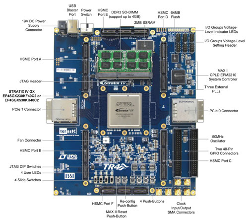
Stratix IV GX EP4SGX530
- 531,200 logic elements (LEs)
- 27,376K total memory Kbits
- 1,024 18x18-bit multipliers blocks
- 4 PCI Express hard IP Blocks
- 744 user I/Os
- 8 phase locked loops (PLLs)
FPGA Configuration
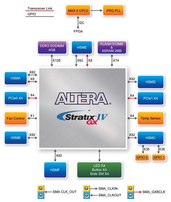
- MAXII CPLD EPM2210 System Controller and Fast Passive Parallel (FPP) configuration
- On-board USB Blaster for use with the Quartus II Programmer
- Programmable PLL timing chip configured via MAX II CPLD
- Supports JTAG mode
Memory Devices
- 64MB Flash with a 16-bit data bus
- 2MB SSRAM (512K x 32)
DDR3 SO-DIMM Socket
- Up to 4GB capacity
- Maximum memory clock rate at 533MHz
- Theoretical bandwidth up to 68Gbps
Buttons, Switches and LEDs
- 4 user-controllable LEDs
- 4 user-defined
- 4 slide switches for user-defined inputs
On-Board Clocks
SMA Connectors
- SMA connector pair for differential clock inputs
- SMA connector pair for differential clock outputs
- SMA connector for clock output
- SMA connector for external clock input
Two PCI Express x4 Connectors
- Support connection speed of Gen1 at 2.5Gbps/lane to Gen2 at 5.0Gbps/lane
- High-speed transceiver channels up to 8.5 Gbps
- Support downstream mode
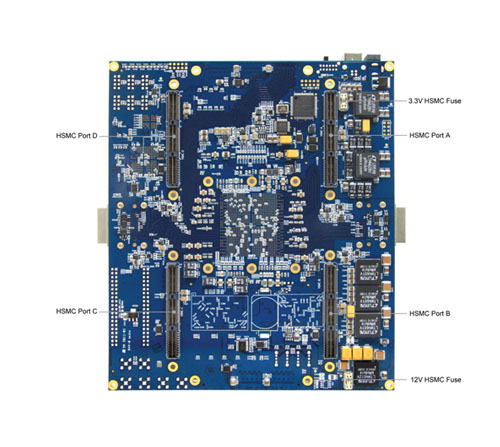
Six 172-pins High Speed Mezzanine Card (HSMC)
- 6 HSMC connectors
- Configurable I/O standards - 1.5V, 1.8V, 2.5V, 3.0V
- Total of 16 high-speed transceivers up to 6.5 Gbps
- 52 true LVDS channels up to 1.6Gbps
- 16 emulated LVDS channels up to 1.1Gbps
Two 40-pin Expansion Headers
- 72 FPGA I/O pins; 4 power and ground lines
- Configurable I/O standards - 1.5V, 1.8V, 2.5V, 3.0V
- Shares pins with HSMC Port
Power
Block Diagram
Download
Documents
| TR4_User_Manual |
- |
11585 |
2012-01-06 |
 |
CD-ROM
| TR4 CD-ROM |
v.1.0.0 |
|
2012-01-06 |
 |
Please note that all the source codes are provided "as is". For further support or modification, please contactTerasic Support and your request will be transferred to Terasic Design Service.More resources about IP and Dev. Kit are available on Altera User Forums.
TR4 Tools
TR4 Control Panel – allows users to access various components on the TR4 board from a host computer.
TR4 Control Panel

TR4 System Builder – a powerful tool comes with the TR4 board. This tool will allow users to create a Quartus II project file on their custom design for the TR4 board. The top-level design file, pin assignments, and I/O standard settings for the TR4 board will be generated automatically by the TR4 System Builder. In addition, through the HSMC connectors you can select various daughter cards in conjunction with the TR4 using the TR4 System Builder.
TR4 System Builder

The generated Quartus II project files include the following:
- Quartus II Project File (.qpf)
- Quartus II Setting File (.qsf)
- Top-Level Design File (.v)
- External PLL Contorller (.v)
- Synopsis Design Constraints file (.sdc)
- Pin Assignment Document (.htm)
TR4 Reference Designs
- Breathing LEDs
- External Clock Generator
- High Speed Mezzanine Card Connector Test
- DDR3 Nios II Read/Write Loopback Test
- DDR3 HDL Read/Write Test
- PCI Express Fundamental Communication
- PCI Express Image Processing Application
The TR4 package includes:

|


