|
|
The Terasic TR10a-HL Arria 10 GX FPGA Development Kit provides the ideal hardware solution for designs that demand high capacity and bandwidth memory interfacing, ultra-low latency communication, and power efficiency. With a full-height, 1/2-length form-factor package, the TR10a-HL is designed for the most demanding high-end applications, empowered with the top-of-the-line Altera Arria 10 GX, delivering the best system-level integration and flexibility in the industry. The Arria® 10 GX FPGA features integrated transceivers that transfer at a maximum of 12.5 Gbps, allowing the TR10a-HL to be fully compliant with version 3.0 of the PCI Express standard, as well as allowing an ultra low-latency, straight connections to four external 40G QSFP+ modules. Not relying on an external PHY will accelerate mainstream development of network applications enabling customers to deploy designs for a broad range of high-speed connectivity applications. For designs that demand high capacity and high speed for memory and storage, the TR10a-HL delivers with six independent banks of QDRII+ SRAM, high-speed parallel flash memory. The feature-set of the TR10a-HL fully supports all high-intensity applications such as low-latency trading, cloud computing, high-performance computing, data acquisition, network processing, and signal processing.
FPGA- Altera Arria 10 GX FPGA (10AX115N2F45E1SG)
FPGA Configuration- On-Board USB Blaster II or JTAG header for FPGA programming
- Fast passive parallel (FPPx32) configuration via MAX II CPLD and flash memory
Memory- 256MB FLASH
- 6 Independent 550 MHz QDRII+SRAMs, 18-bits data bus and 72Mbit for each ( * )
Communication and Expansion- Four QSFP+ connectors
- PCI Express (PCIe) x8 edge connector (includes Windows PCIe drivers)
- One 2x5 RS422 expansion header
- One 2x4 GPIO expansion header
Others- General user input / output:
- 4 LEDs
- 1 Bracket LED Array
- 4 push-buttons
- 2 DIP switches
- On-Board Clock
- 50MHz Oscillator
- Programmable Clock Generator
- System Monitor and Control
- Temperature sensor
- Power Monitor
- Fan control
- Power
- PCI Express 6-pin power connector, 12V DC Input
- PCI Express edge connector power
- Mechanical Specification
- PCI Express standard height and 1/2-length
Block Diagram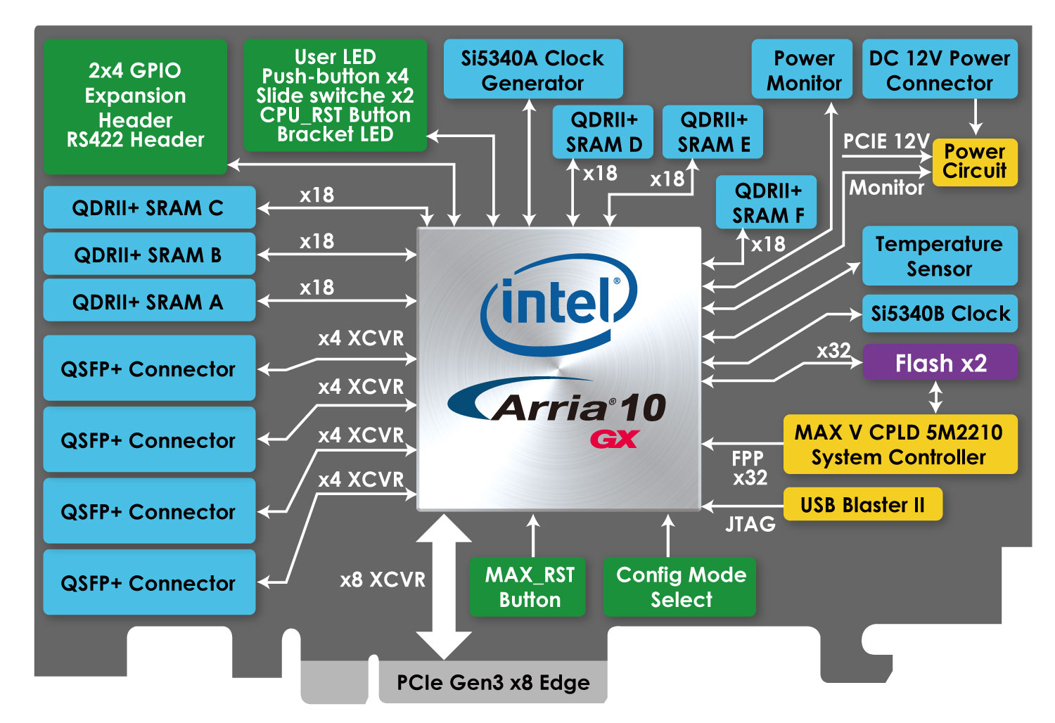
Documents| TR10a-HL User Manual | 1.0.2 | 6642 | 2019-04-18 |  |
CD-ROM| TR10a-HL CD-ROM | 1.0.2 | | 2019-04-18 | |

- TR10a-HL Development Board
- TR10a-HL Quick Start Guide
- Micro USB Cable
- Screw & Copper Pillar Package
- Fan (Installed)
- AC Power Cord
- Power Supply & Power Cable
- PCIe Bracket (Installed)
Quartus design software license is not included in this kit.
|
|
|


