Terasic TR5 FPGA Development Board
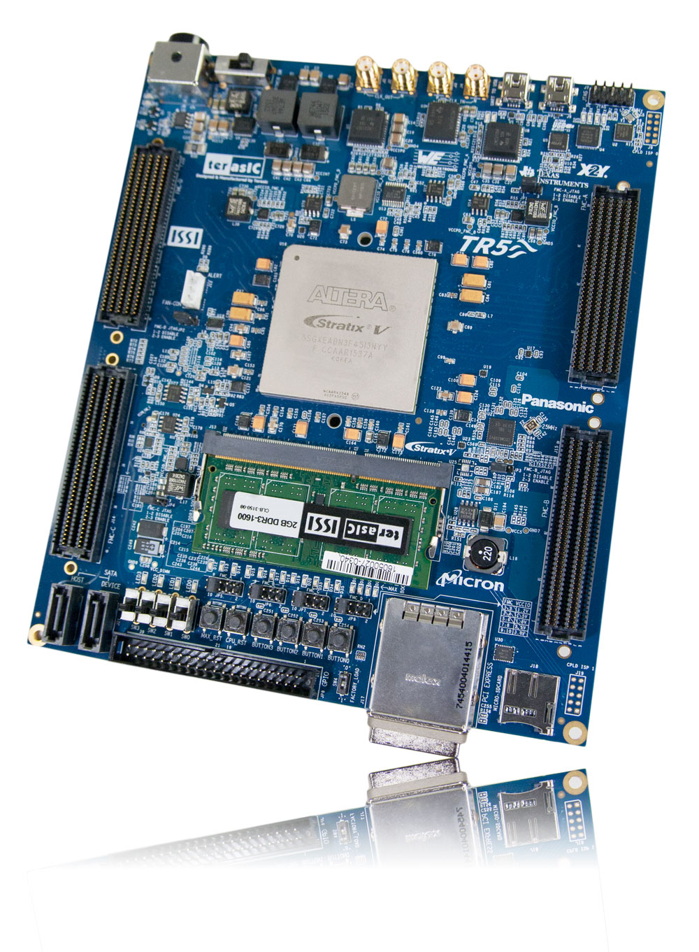
 TR5 FPGA development board using the Altera Stratix V GX FPGA provides high-speed operation and transmission with large capacity up to 952K LE.
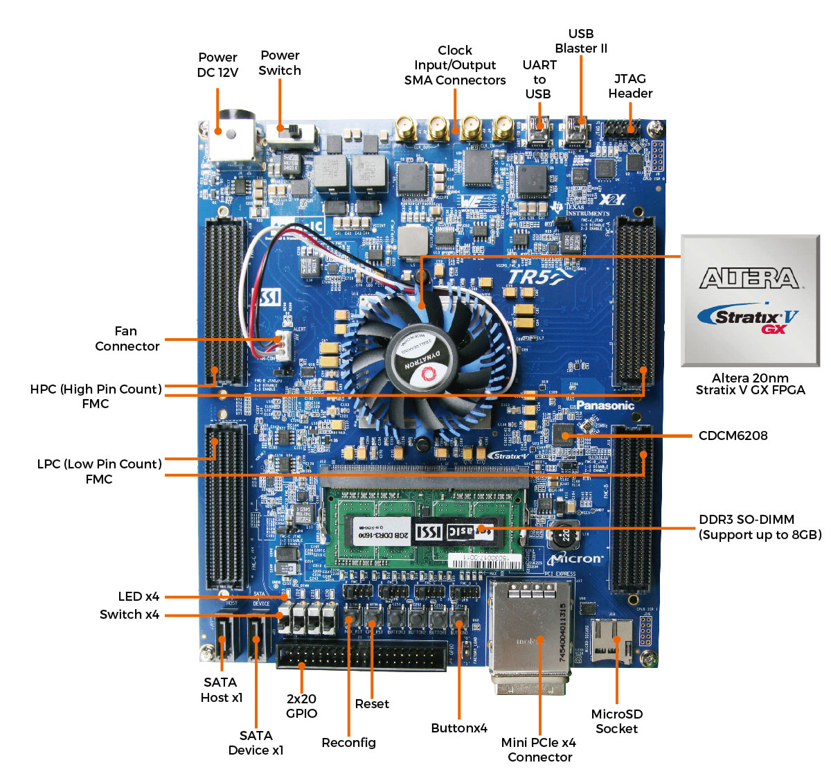
The board provides four FMC connectors and a 2x20 GPIO connector. It offers a total of more than 500 I/Os for users to expand the usage with the peripherals connected. There are built-in high-speed DDR3 memory and SSRAM to increase the bandwidth for accessing large amounts of data for high-speed computation. In addition, the board also has PCIe and SATA interfaces for high-speed data transmission.
The main applications of TR5 are ASIC prototyping validation and the establishment of prototype systems. The FMC connectors onboard are standard interfaces. Users can purchase or develop various FMC daughter cards to expand their system. For developers who need to use multiple FPGAs, they can leverage Terasic’s FMC or PCIe cable to establish an inter-stackable multi-boards communication system. Users can also purchase Terasic PCIe daughter card to communicate with host PC.
 The TR5 development kit includes a variety of reference design examples for peripherals such as DDR3 SDRAM, SD card, USB-to-UART, SATA, PCIe, and an FMC connector. The kit is user friendly and enables users to quickly get started or verify the functions. The kit also provides a tool named "System Builder" software. It can automatically generate a complete Quartus project including pin assignment and clock configuration IP upon users' selections of peripherals, FMC daughter cards, and a designated clock frequency. It helps users avoid time-consuming and error-prone manual pin-assignment work.
Power and Clock Solution
 | Memory Solution
 | X2Y Power Decoupling Solution
 |
| | | |
Inductive Component Solution

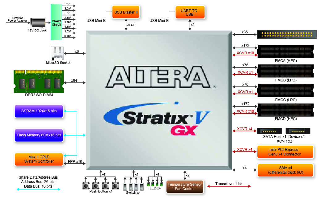
FPGA Device 5SGXEA7N2F45C2N- 622K Logic Elements (LEs)
- 57.16 Mbits Memory
- 256 Variable-precision DSP Blocks
- 512 18x18-bit Multipliers Blocks
- 28 Fractional PLLs and 4DLLs
- *FPGAs with higher LEs are also available. Please contact Terasic sales team.
FPGA Configuration- MAX II CPLD EPM2210 System Controller for Fast Passive Parallel (FPP x16) Configuration
- On-board USB-Blaster II for use with Quartus II Programmer
Memory
- 128MB Flash with a 16-bit Data Bus
- 2MB SSRAM (1M x 16)
DDR3 SO-DIMM Socket
- Up to 8GB Capacity
- Maximum Clock Rate at 933 MHz
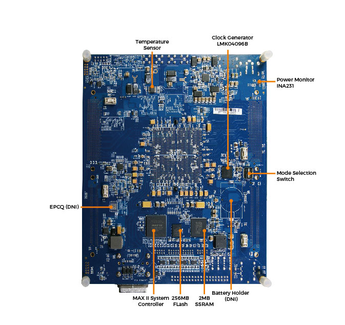
On-board Clocks
- 50 MHz Fixed Oscillator
- CDCM6208 Programmable PLL
- LMK04906B Programmable PLL
SMA Connectors
- SMA Connector Pair for Differential Clock Input and Output
Buttons, Switches and LEDs
- 4 User-controllable LEDs
- 4 Buttons for User-defined Inputs
- 4 Slide Switches for User-defined Inputs
Mini PCI Express Gen 2x4 Connector
- Support PCI Express Gen2 x4 (5.0Gbps/lanes)
- High-speed Transceiver Channels up to 5 Gbps
- Support Downstream Mode
Four FPGA Mezzanine Card (FMC) Connectors
- 2 HPC (high-pin count) FMC connectors up to 172 x2 Single-end I/O, 2 LPC (low-pin count) FMC connectors up to 76 x2 Single-end I/O
- 10 Transceiver Channels for each HPC FMC connector and 1Transceiver Channel for LPC each HPC FMC connector
- FMC VITA 57.1 Compliant
- Adjustable VADJ : 1.2V/1.5V/1.8V/2.5V/3.0V.
One 40-pin Expansion Header- 36 FPGA I/O pins; 4 power and ground lines
- I/O standards: 3.3V
Power
Block Diagram
 Expansion with FMC ConnectorConnect to the FMC daughter cards: SDI-FMC, XTS-FMC and HDMI-FMC 
Connect to the D8M-FMC FMC daughter card 
Connect to TI JESD board through Terasic JESD-FMC adapter card 
Board to board connection through FMC cable 
Expansion with PCI Express Cabling ConnectorConnect to PC with PCIe Cabling and Terasic PCA adapter card 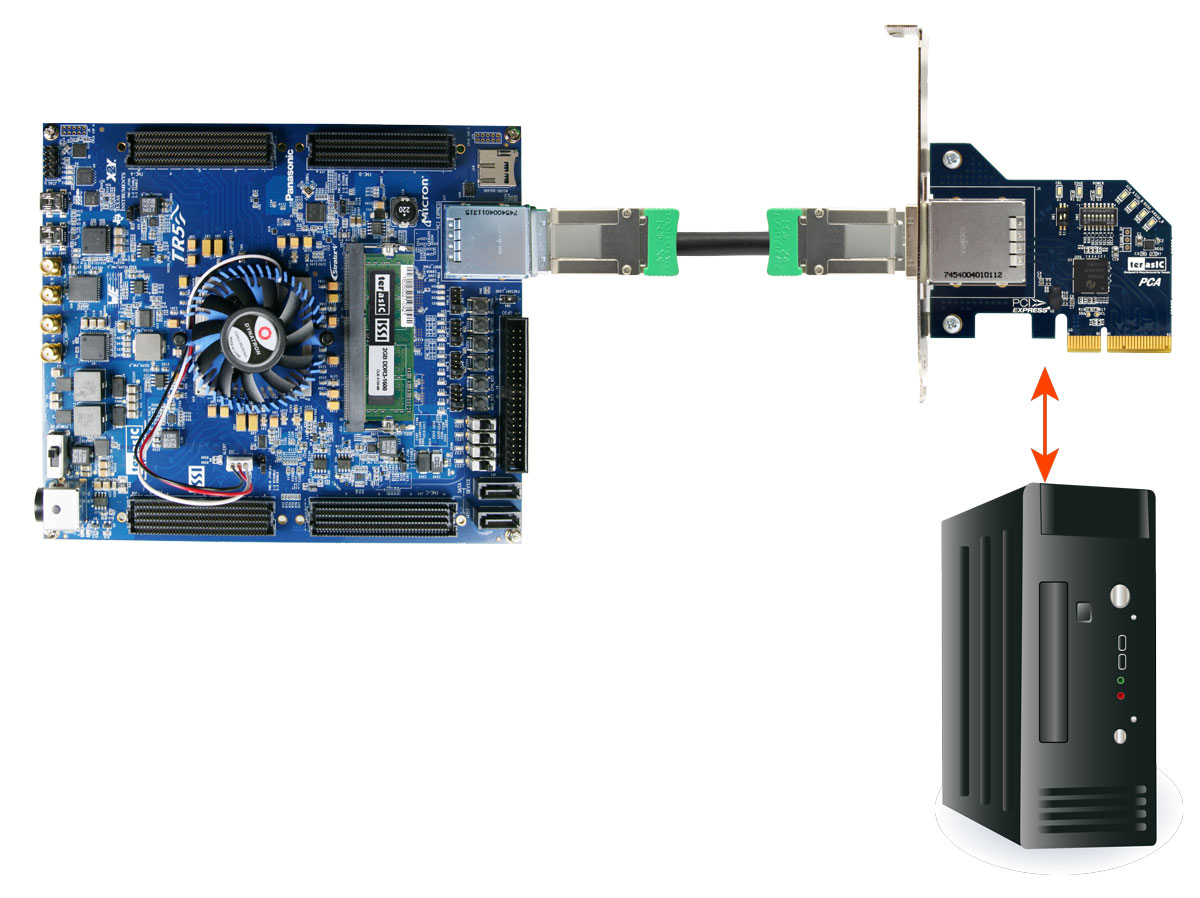
Board to board connection through PCIe Cable 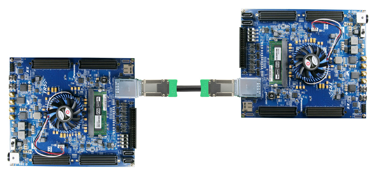
Expansion with SATA ConnectorBoard to board connection through SATA cable 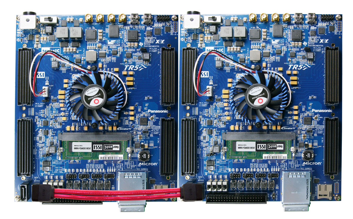
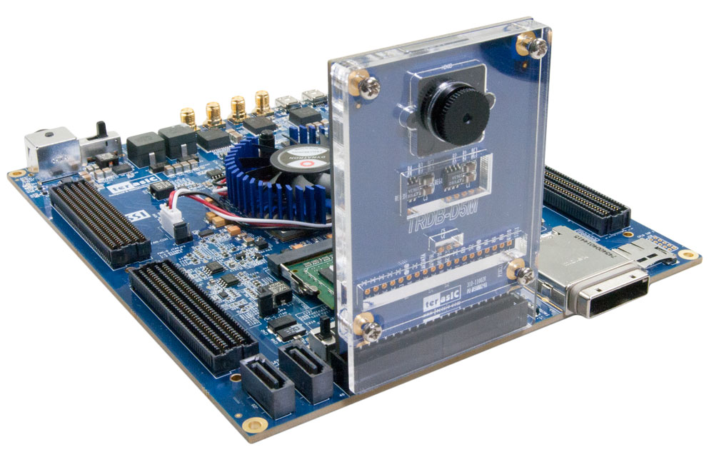
Expansion with GPIO ConnectorConnect to the D5M daughter card
Connect to the MTL2 daughter card
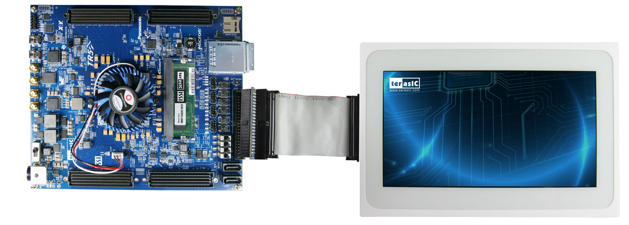
Connect to the LT24 daughter card 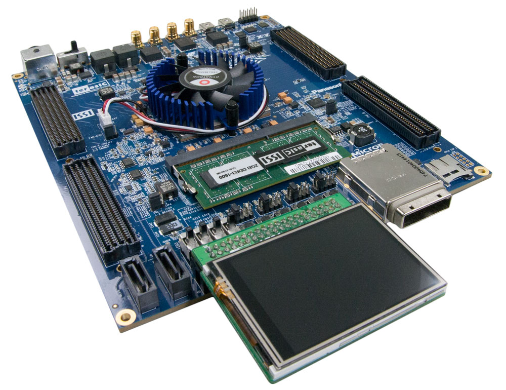
Size:160.8 x 188.5 mm Document| TR5 User Manual | 1.0.0 | 7673 | 2016-10-04 |  |
CD-ROM| TR5 CD-ROM | 1.0.0 | | 2016-10-04 |  |
Please note that all the source codes are provided "as is". For further support or modification, please contact Terasic Support and your request will be transferred to Terasic Design Service.More resources about IP and Dev. Kit are available on Altera User Forums. TR5 ToolsTR5 System Builder – This is a powerful tool that comes with the TR5 board. This tool allows users to create a Quartus II project for their custom design on TR5 board. The top-level design file, pin assignments, and I/O standard settings for TR5 board can be generated automatically by the TR5 System Builder. Users can also select various daughter cards in conjunction with TR5 via FMC connectors using the TR5 System Builder.

TR5 Reference Designs- Breathing LEDs
- Configuration for External Clock Generator
- Flash, SSRAM and SD Card Test Code based on Nios II
- Fan Control and Temperature Monitor
- Communication with Host PC through UART-to-USB
- Parallel Flash Loader
- DDR3 Nios II Read/Write Loopback Test
- DDR3 HDL Read/Write Test
- Loopback Test for FPGA Mezzanine Card (FMC) Connector
- PCI Express Fundamental Communication
- PCI Express Image Processing Application
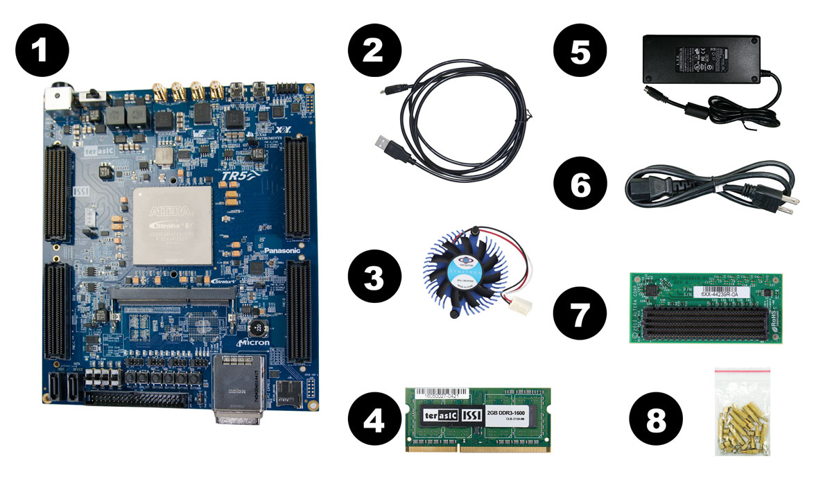
Quartus design software license is not included in this kit. The TR5 package includes:- TR5 FPGA Development Board
- Type A to Mini-B USB Cable
- Fan (Installed)
- 2GB DDR3-1600 SO-DIMM Module (Installed)
- 12V DC Power Supply
- AC Power Cord
- FMC Loopback Card
- Screws, Copper Stands, and Silicon Footstands
| Capacitive Component Solution
 | Flash Solution 
|


