|
|
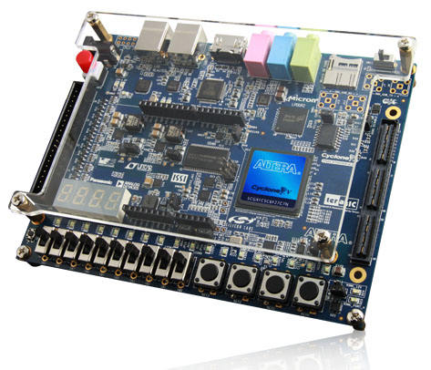
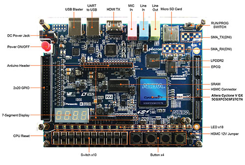
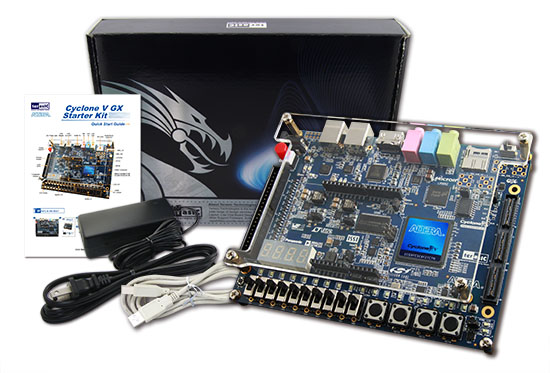
The Cyclone V Starter Kit presents a robust hardware design platform built around the Altera Cyclone V GX FPGA, which is optimized for the lowest cost and power requirement for transceiver applications with industry-leading programmable logic for ultimate design flexibility. With Cyclone V FPGAs, you can get the power, cost, and performance levels you need for high-volume applications including protocol bridging, motor control drives, broadcast video converter and capture cards, and handheld devices. The Cyclone V Starter Kit development board includes hardware such as Arduino Header, on-board USB Blaster, audio and video capabilities and much more. In addition, an on-board HSMC connector with high-speed transceivers allows for an even greater array of hardware setups. By leveraging all of these capabilities, the Cyclone V Starter Kit is the perfect solution for showcasing, evaluating, and prototyping the true potential of the Altera Cyclone V GX FPGA. FPGA Device- Cyclone V GX 5CGXFC5C6F27C7N Device
- 77K Programmable Logic Elements
- 4884 Kbits embedded memory
- Six Fractional PLLs
- Two Hard Memory Controllers
- Six 3.125G Transceivers
Configuration and Debug- Quad Serial Configuration device – EPCQ256 on FPGA
- On-Board USB Blaster (Normal Type-B USB connector)
- JTAG and AS mode configuration supported
Memory Device- 4Gb LPDDR2 x32 bits data bus
- 4Mb SRAM x16 bits data bus
CommunicationExpansion I/O- HSMC x 1, including 4-lanes 3.125G transceiver
- 2x20 GPIO Header
- Arduino header, including analog pins
- SMA x 4 (DNI), one-lane 3.125G transceiver
Display- HDMI TX, compatible with DVI v1.0 and HDCP v1.4
Audio- 24-bit CODEC, Line-in, line-out, and microphone-in jacks
Switches, Buttons, LED, and 7-Segments- 18 LEDs
- 10 Slide Switches
- 4 Debounced Push Buttons
- 1 CPU reset Push Buttons
- Four 7-Segments
Micro SD Card Socket- Provides SPI and 4-bit SD mode for SD Card access
ADC- 12-Bit Resolution, 500Ksps Sampling Rate. SPI Interface.
- 8-Channel Analog Input. Input Range : 0V ~ 4.096V.
PowerBlock Diagram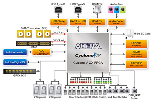
Daughter Card Demonstations
Documents| C5G User Manual | 1.2.1 | 10756 | 2014-04-07 |  |
CD-ROM| C5G System CD-ROM | 1.2.1 | | 2014-06-24 | 
|
|
|
|


